* On your first PCB Assembly order!
* Up to $300 discount
 C - A L L E Y
 Home | Events | PCB | About Us | News | Contact Us
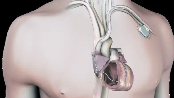
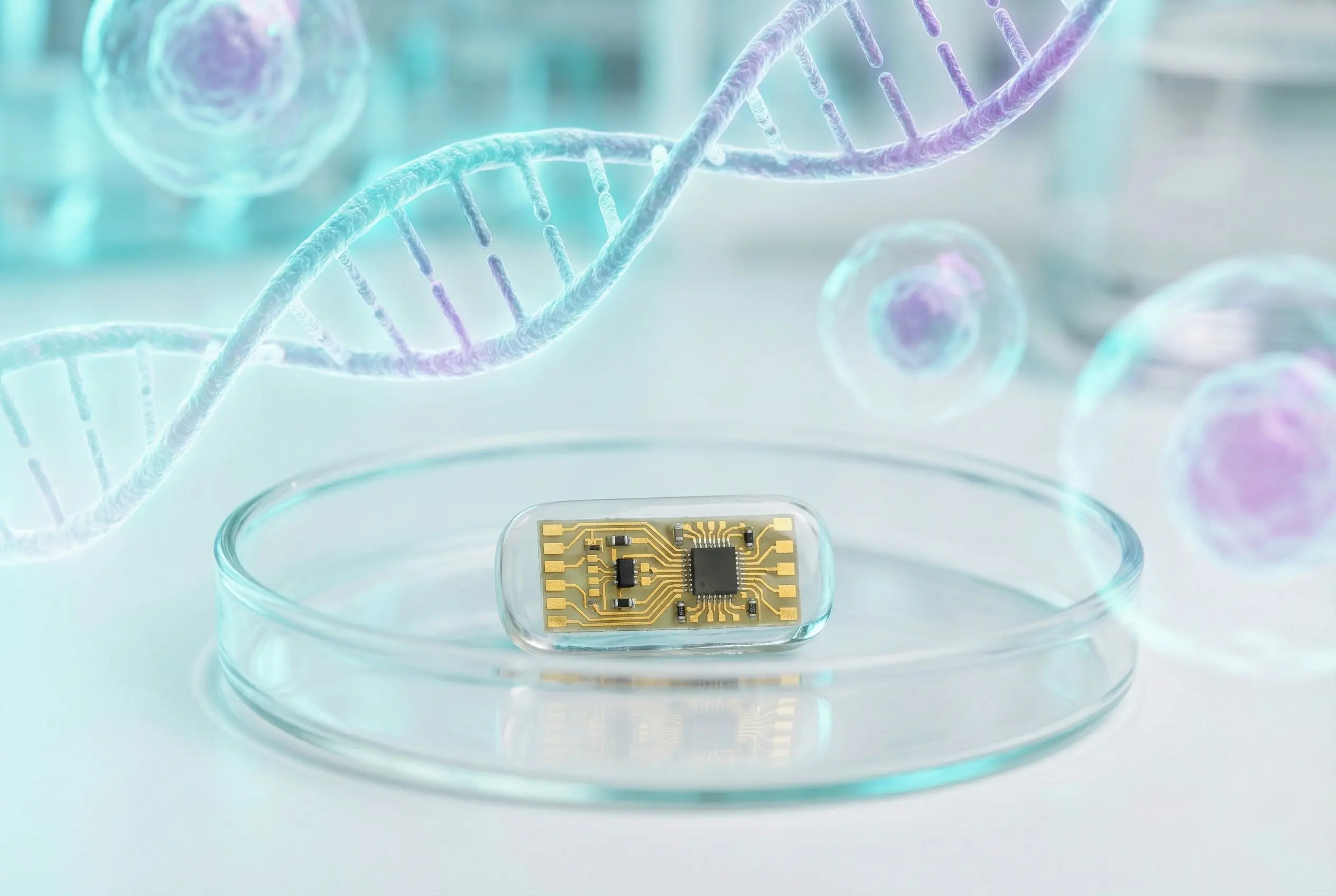
Implantable medical devices include cardiac pacemakers, neurostimulators, drug pumps, and cochlear implants. The core electronic control systems of these devices rely on micro printed circuit board assemblies. The micro PCBA assembly process faces multiple technical challenges, involving material selection, soldering precision, reliability, and cleanliness control.
I. Physical Assembly Constraints from Miniaturization
1. Component Size and Placement Accuracy
The passive components used in implantable devices are typically 01005 or 008004 size. An 010005 component measures 0.4mm × 0.2mm, while an 008004 component measures 0.25mm × 0.125mm. The placement accuracy of standard pick-and-place machines ranges from ±25μm to ±50μm. For 008004 components, this accuracy range approaches 20% of the component size. Placement deviation exceeding 25% of the component width can lead to solder bridging or opens.
Solutions include using pick-and-place machines with closed-loop feedback, employing high-resolution vision positioning systems, and adding post-placement automated optical inspection.
2. Substrate Design and Manufacturing Tolerances
Micro PCBAs typically use 2- to 4-layer HDI boards with line/space controlled below 50μm. Laser-drilled microvias range from 75μm to 100μm in diameter. During multilayer lamination, cumulative layer-to-layer registration deviation can reach ±30μm, causing misalignment between buried vias and receiving pads. This requires reserving sufficient annular rings at the design stage and adopting direct imaging photolithography instead of traditional exposure.
II. High-Reliability Soldering and Interconnection Challenges
1. Miniaturized Solder Joints and Mechanical Strength
Implantable devices undergo body movement, temperature changes, and shock. A single solder joint diameter can be as small as 150μm. In miniaturized solder joints, the proportion of intermetallic compound formed by conventional SAC305 solder relative to the joint volume increases, leading to increased brittleness. Countermeasures include using low-silver solder paste doped with manganese or manganese, controlling peak reflow temperature between 240°C and 245°C, and limiting dwell time to 30 to 50 seconds. Additionally, using transient liquid phase sintering technology to create all-intermetallic copper-tin solder joints can increase shear strength to 1.5 times that of SAC305 solder joints.
2. Gold Embrittlement Control
Many implantable PCBAs use ENIG surface finish. Nickel layer thickness is 3 to 6μm, gold layer thickness 0.05 to 0.1μm. Multiple reflow cycles cause the gold layer to fully diffuse into the solder, forming needle-like AuSn4 intermetallic compounds. When the gold concentration in the solder joint exceeds 3wt%, the joint shows significant brittleness. Control methods include limiting ENIG gold layer thickness to no more than 0.08μm, reducing the number of reflow cycles to no more than two, or using ENEPIG (nickel-palladium-gold) finish on critical areas, where the palladium layer prevents gold diffusion.
III. Cleanliness and Biocompatibility Requirements
1. Ionic Contaminant Control
Ionic residues on implantable PCBAs can lead to electrochemical migration and metal corrosion. When surface insulation resistance drops below 1MΩ, the device may malfunction. Common contaminants include halides and acids from flux residues.
Process control standards: Use low-solid, no-clean flux, but cleaning must still be performed. Post-batch ionic contaminant testing per IPC-TM-650 2.3.28 requires ionic equivalent NaCl below 0.5μg/cm². Employ in-line plasma cleaning processes to remove residues from fine crevices.
2. Material Biocompatibility
PCBA materials must pass ISO 10993 series tests. Standard FR-4 contains brominated flame retardants and is not accepted by human tissue. Alternative materials are liquid crystal polymer and polyimide substrates, paired with medical-grade coverlays. Lead content in solder must be below 0.1wt%, meeting RoHS requirements while passing cytotoxicity tests. Hermetic enclosure materials use titanium or ceramic. The PCBA must accommodate the sealing temperature profiles of these materials, typically 250°C to 300°C.
IV. Manufacturing Process Verification and Traceability
1. Full-Process Inspection Coverage
Hidden solder joints on micro PCBAs, such as underfill areas of wafer-level chip-scale packages and interconnects within multi-chip modules, cannot be inspected optically. Use 3D X-ray laminography systems with resolution capability below 5μm. X-ray inspection data for each individual PCBA must be retained for no less than 10 years.
2. Closed-Loop Process Parameter Control
Reflow ovens require real-time oxygen concentration monitoring and temperature profile verification systems. A thermal profiling board is used before each shift to collect data. An automatic alarm is triggered when data deviation exceeds ±2°C. Pick-and-place machine nozzles use ceramic materials to reduce electrostatic damage. Each batch's production records include placement force feedback data, solder paste print thickness maps, and real-time temperature profiles for each zone of the reflow oven.
Summary
The assembly of micro PCBAs for implantable medical devices presents clear challenges in component placement, solder joint reliability, cleanliness control, and process verification. Addressing these challenges requires introducing design-for-manufacturability analysis from the design phase, using high-precision equipment and in-line monitoring during production, and performing rigorous cleanliness testing and X-ray inspection at the back end. For a PCBA manufacturing facility, obtaining relevant certifications for implantable medical applications and building the above capabilities is a necessary condition to enter this high-end market.
With 17 years of expertise in PCBA design, manufacturing, and service, KingshengPCBA is ready to help turn your ideas into reality. Feel free to contact us anytime to discuss your requirements and get a professional quotation.

Please send Email to kspcba@c-alley.com or call us through +86 13828766801 Or submit your inquiry by online form. Please fill out below form and attach your manufacturing files( PCB Gerber files and BOM List) if need quotation. We will contact you shortly.
 +86 13828766801
 kspcba@c-alley.com
 https://www.kingshengpcba.com/
 2/F, Building 6, Tangtou 3rd Industrial Zone, Tangtou Community, Shiyan Town, Baoan District, Shenzhen, China, 518108
We would also like to thank our customers for their trust and support. The company's outstanding achievements are mainly due to the loyalty of our customers, which also encourages and spurs our company to forge ahead.


