* On your first PCB Assembly order!
* Up to $300 discount
 C - A L L E Y
 Home | Events | PCB | About Us | News | Contact Us
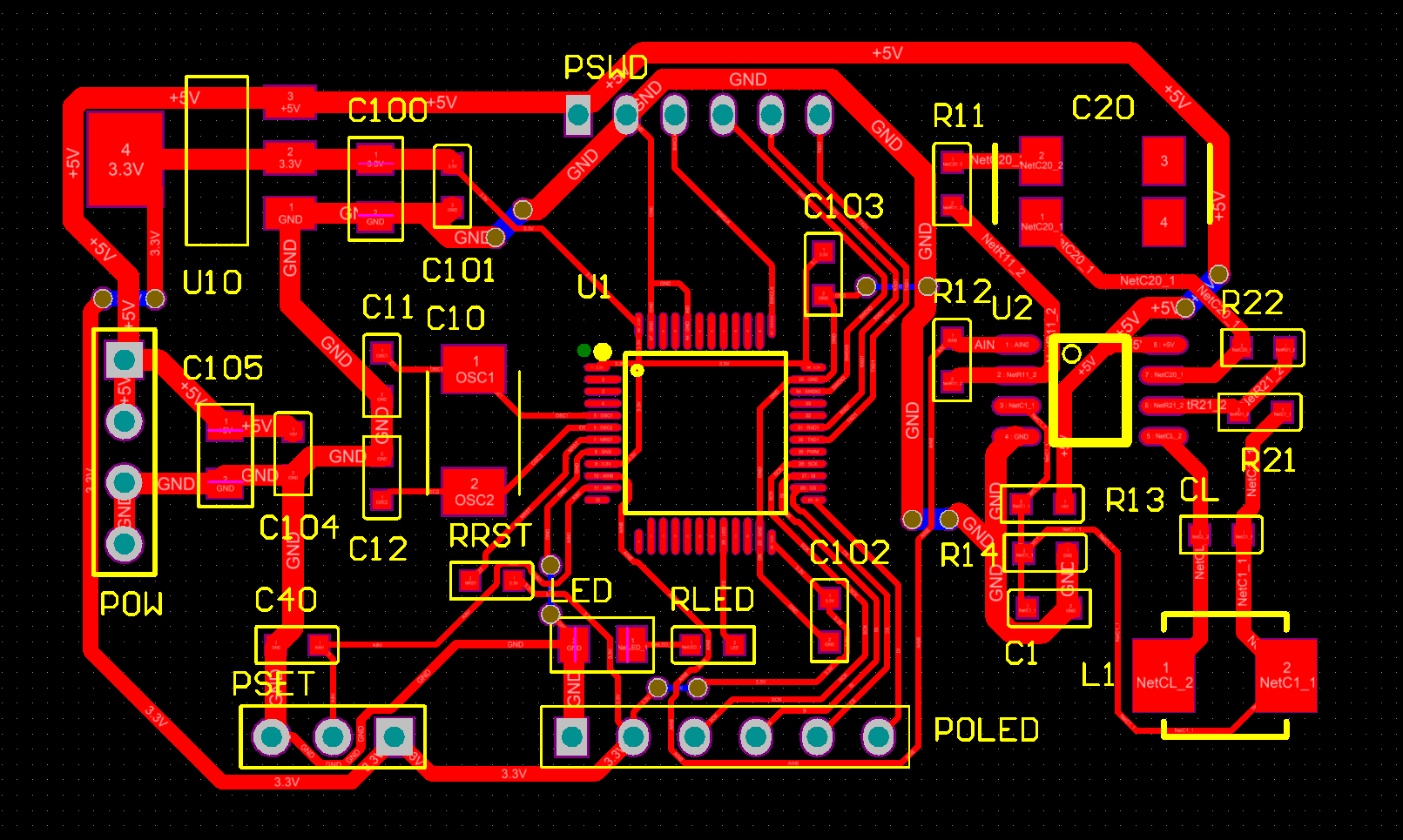
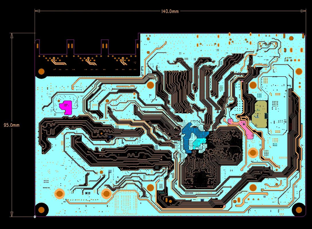
In the era of IoT, 5G, and AI-driven devices, the race to pack more functionality into smaller form factors has made PCB density optimization a critical focus for designers and manufacturers. For PCBA factories, achieving space efficiency without compromising performance requires a multi-disciplinary approach—balancing electrical, thermal, and mechanical constraints. Below, we break down the key strategies to master high-density PCB design.
I. Leveraging HDI Technology: The Backbone of Miniaturization
High-Density Interconnect (HDI) PCBs are no longer optional for complex designs. By utilizing laser-drilled microvias (≤100µm), stacked vias, and fine-pitch traces (≤3/3mil), HDI allows:
① 30–50% reduction in board area compared to conventional PCBs.
② Improved signal integrity with shorter interconnects, critical for high-speed protocols like DDR5 or PCIe Gen6.
③ Fewer layers, reducing cost and weight (e.g., 8-layer HDI can replace 12+ layers of traditional PCB).
Design Tip: Combine any-layer via technology with low-loss materials (e.g., Megtron 6) for RF/microwave applications.
II. Component Selection & Placement: Beyond Miniaturization
A. Advanced Packaging
① Chip-Scale Packages (CSP): 0.4mm pitch BGAs or wafer-level packages (WLP) save 60% space vs. QFNs.
② 01005 passives: Ideal for wearables but require precision placement (±15µm accuracy).
B. Embedded Components
① Embedded actives/passives: Resistors/capacitors buried in layers free up surface area.
② Trade-off: Higher fabrication costs (~20–30% increase) but ideal for aerospace/medical devices.
C. 3D Component Stacking
PoP (Package-on-Package): Memory + logic stacking reduces footprint (e.g., mobile SoCs).
III. Routing & Layout: Maximizing Real Estate
① Via-in-Pad: Eliminates stubs and saves space but requires filled and capped vias to prevent solder wicking.
② Differential Pair Routing: Tight coupling (3W rule) for 56Gbps+ interfaces (e.g., USB4).
③ Flex-Rigid Hybrids: Bendable sections enable compact 3D assemblies (e.g., foldable smartphones). Critical Consideration: Use simulation tools (e.g., HyperLynx) to model EMI/thermal hotspots early.
IV. Thermal & Signal Integrity Management
A. Heat Dissipation
① Micro-via arrays: Under high-power ICs (e.g., FPGAs) improve thermal resistance by 40%.
② Metal-core PCBs: For LED/automotive applications with >10W/cm² heat flux.
B. Signal Integrity
① Controlled impedance: Tight tolerances (±5%) for mmWave frequencies (e.g., 28GHz 5G).
② Ground plane partitioning: Isolate noisy digital/RF sections to reduce crosstalk.
V. Design-for-Manufacturing (DFM) Collaboration
Close coordination with your PCBA partner ensures:
① Avoiding tombstoning: Symmetric pad designs for 0201/01005 components.
② Testability: Embedded test points or boundary-scan (JTAG) for high-density boards.
③ Material selection: Low-CTE substrates (e.g., Arlon 85N) for reliability in thermal cycling.
VI: Conclusion: The Future of High-Density PCBs
As edge computing and AR/VR push size limits further, innovations like substrate-like PCBs (SLP) and additive manufacturing will redefine density benchmarks. At [Your Company Name], we combine advanced process capabilities (e.g., 25µm laser drilling) with DFM expertise to turn complex designs into manufacturable solutions.
With 17 years of expertise in PCBA design, manufacturing, and service, KingshengPCBA is ready to help turn your ideas into reality. Ready to optimize your next design? Feel free to contact us anytime to discuss your requirements and get a professional quotation.

Please send Email to kspcba@c-alley.com or call us through +86 13828766801 Or submit your inquiry by online form. Please fill out below form and attach your manufacturing files( PCB Gerber files and BOM List) if need quotation. We will contact you shortly.
 +86 13828766801
 kspcba@c-alley.com
 https://www.kingshengpcba.com/
 2/F, Building 6, Tangtou 3rd Industrial Zone, Tangtou Community, Shiyan Town, Baoan District, Shenzhen, China, 518108
We would also like to thank our customers for their trust and support. The company's outstanding achievements are mainly due to the loyalty of our customers, which also encourages and spurs our company to forge ahead.


