* On your first PCB Assembly order!
* Up to $300 discount
 C - A L L E Y
 Home | Events | PCB | About Us | News | Contact Us
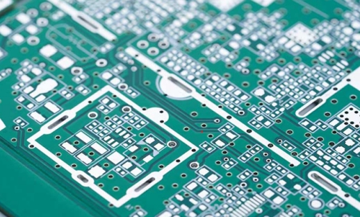
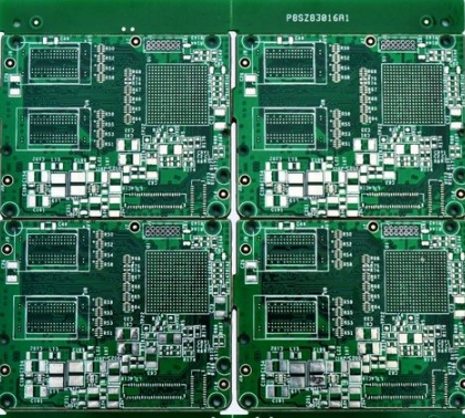
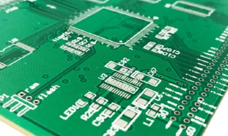
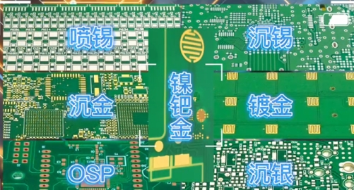
In the world of printed circuit board (PCB) manufacturing, selecting the right surface finish is a critical decision that impacts performance, reliability, and longevity. As a leading PCBA manufacturer, we understand that the surface finish serves as the interface between components and the bare PCB, protecting copper traces from oxidation while ensuring optimal solderability. With increasing demands for miniaturization, high-frequency operation, and harsh-environment reliability, choosing the appropriate finish has never been more important. This 2000-word guide explores all major PCB surface finish options, their comparative advantages, and how to select the ideal solution for your application.

I: Understanding PCB Surface Finishes: Purpose and Key Considerations
PCB surface finishes serve three primary functions:
Protecting exposed copper from oxidation and corrosion Providing a solderable surface for component attachment Maintaining electrical connectivity throughout the product's lifecycle When selecting a finish, engineers must evaluate:
① Solderability: How well the finish facilitates reliable solder joints
② Durability: Resistance to environmental factors like humidity, temperature cycling
③ Cost: Material and processing expenses
④ Lead-free compliance: Adherence to RoHS and other regulations
⑤ Signal integrity: Critical for high-frequency applications
⑥ Assembly compatibility: Suitability for SMT, through-hole, or mixed technologies
II:Comprehensive Analysis of PCB Surface Finish Options
1. Hot Air Solder Leveling (HASL)
The traditional HASL process involves dipping PCBs in molten solder (traditionally tin-lead, now mostly lead-free SAC alloys) followed by hot air leveling.
Advantages:
① Lowest cost option (0.05−0.05−0.15 per square inch)
② Excellent solderability with wide process window
③ Thick coating (2-5μm) provides good shelf life (12+ months)
Limitations:
① Not suitable for fine-pitch components (<0.5mm pitch)
② Thermal shock from process can warp thin PCBs
③ Uneven surface topography challenges HDI designs
Best for: Consumer electronics, cost-sensitive applications where fine features aren't required.
III: Comprehensive Analysis of PCB Surface Finish Options
1. Hot Air Solder Leveling (HASL)
The traditional HASL process involves dipping PCBs in molten solder (traditionally tin-lead, now mostly lead-free SAC alloys) followed by hot air leveling.
Advantages:
① Lowest cost option (0.05−0.05−0.15 per square inch)
② Excellent solderability with wide process window
③ Thick coating (2-5μm) provides good shelf life (12+ months)
Limitations:
① Not suitable for fine-pitch components (<0.5mm pitch)
② Thermal shock from process can warp thin PCBs
③ Uneven surface topography challenges HDI designs
Best for: Consumer electronics, cost-sensitive applications where fine features aren't required.
2. Immersion Silver (IAg)
A thin (0.1-0.3μm) silver layer deposited directly on copper through displacement reaction.
Advantages:
① Excellent high-frequency performance
② Good solderability with wide process window
③ Lower cost than ENIG
④ Suitable for fine-pitch components
Limitations:
① Prone to tarnishing (requires careful packaging)
② Limited shelf life (6-9 months)
③ Not suitable for wire bonding
Best for: RF/microwave applications, automotive electronics where cost/performance balance is key.
3. Electroless Nickel Electroless Palladium Immersion Gold (ENEPIG)
Three-layer structure: nickel (3-6μm), palladium (0.05-0.1μm), and gold (0.03-0.05μm).
Advantages:
① Eliminates black pad risk of ENIG
② Superior wire bonding capability
③ Excellent shelf life (12+ months)
④ Withstands multiple reflow cycles
Limitations:
① Highest cost finish option
② Complex process control required
③ Overkill for many standard applications
Best for: Advanced packaging, military/aerospace, and high-reliability medical devices.
IV: Emerging Trends in PCB Surface Finishes
Nanocoating Technologies:
Atomic-layer deposition (ALD) of ultra-thin protective films (<100nm) that maintain solderability while preventing oxidation.
Hybrid Finishes: Combining advantages of different finishes, such as selective ENIG on contact areas with OSP elsewhere to optimize cost/performance.
Sustainable Chemistry: Development of bio-based OSP formulations and reduced gold thickness in ENIG to lower environmental impact.
High-Temperature Finishes: New alloys and coatings for extreme environment applications like downhole drilling (200°C+ operation).
V:Selection Methodology: Choosing the Right Finish
Follow this decision framework: Define Application Requirements:
① Operating environment (temperature, humidity, chemical exposure)
② Expected product lifetime
③ Signal frequency requirements
④ Component types and pitches
Evaluate Manufacturing Factors:
① Number of reflow cycles needed
② Secondary operations (press-fit, wire bonding)
③ Rework expectations
Consider Supply Chain Factors:
① Expected time between PCB fabrication and assembly
② Storage and handling conditions
③ Regional environmental regulations
Perform Cost-Benefit Analysis:
① Initial PCB cost vs. potential field failures
② Assembly yield implications
③ Long-term reliability costs
V: Conclusion: Balancing Performance with Practical Considerations
Selecting the optimal PCB surface finish requires careful consideration of technical requirements, manufacturing processes, and total cost of ownership. While ENEPIG offers the most comprehensive performance, its high cost makes it impractical for many applications. Conversely, OSP provides an economical solution for high-density designs but may compromise long-term reliability.
As a PCBA manufacturer with decades of experience, we recommend:
① For consumer electronics: OSP or immersion silver for cost-effective performance
② For automotive/industrial: ENIG or immersion tin for durability
③ For RF/microwave: Immersion silver or carefully controlled ENIG
④ For high-reliability systems: ENEPIG despite higher initial cost The ideal approach involves collaborating with your PCB manufacturer early in the design phase to select a finish that balances all factors. With proper selection and process control, the surface finish will enhance rather than limit your product's performance and durability..
With 17 years of expertise in PCBA design, manufacturing, and service, KingshengPCBA is ready to help turn your ideas into reality. Feel free to contact us anytime to discuss your requirements and get a professional quotation.

Please send Email to kspcba@c-alley.com or call us through +86 13828766801 Or submit your inquiry by online form. Please fill out below form and attach your manufacturing files( PCB Gerber files and BOM List) if need quotation. We will contact you shortly.
 +86 13828766801
 kspcba@c-alley.com
 https://www.kingshengpcba.com/
 2/F, Building 6, Tangtou 3rd Industrial Zone, Tangtou Community, Shiyan Town, Baoan District, Shenzhen, China, 518108
We would also like to thank our customers for their trust and support. The company's outstanding achievements are mainly due to the loyalty of our customers, which also encourages and spurs our company to forge ahead.


