* On your first PCB Assembly order!
* Up to $300 discount
 C - A L L E Y
 Home | Events | PCB | About Us | News | Contact Us
Instrument PCBA Precision Control: Core Essentials of High-Precision Manufacturing from a Third-Party Technical Perspective As the "sensory core" of industrial monitoring, medical detection, and scientific measurement, the PCBA (Printed Circuit Board Assembly) directly determines the measurement accuracy, signal drift, noise level, and batch consistency of the entire system. Particularly in scenarios involving microvolt-level small signal acquisition, high-sensitivity detection, and ultra-low-noise amplification, any subtle deviation in the manufacturing process may lead to data distortion, long-term drift, or false alarms, ultimately affecting decision accuracy and system safety. From a third-party technical service perspective, the core competitiveness of instrument-grade PCBA lies not in the advantage of a single link, but in the integration of full-chain capabilities spanning materials science, precision processes, noise suppression, and quality verification. The following sections provide an in-depth analysis of the manufacturing essentials for high-precision instrument PCBA from four dimensions.
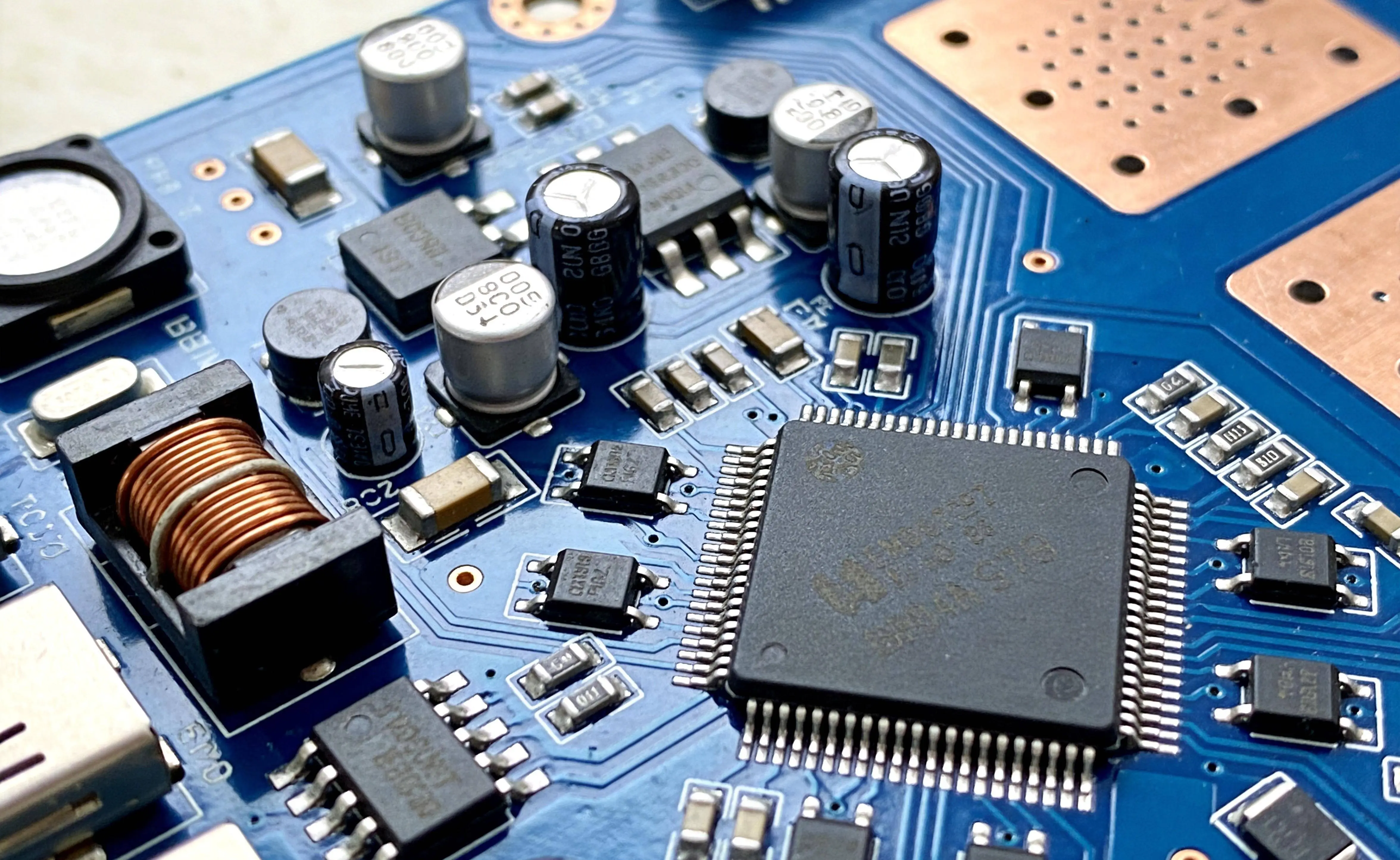
I. PCB Material Selection: Building the Foundational Physical Basis for Precision
1.1 High-Stability PCB Substrate Materials
Instruments often process weak signals at the microvolt or even nanovolt level. The electrical characteristics of PCB materials directly impact signal integrity. High glass transition temperature (High Tg), low dielectric loss (Low Df), and low moisture absorption substrate materials must be employed to ensure stable impedance, minimal signal attenuation, and consistent dielectric constant across wide temperature ranges, fundamentally suppressing temperature drift and signal distortion.
1.2 Rigorous Selection of Instrumentation-Grade Components
Critical components such as operational amplifiers, voltage references, analog-to-digital converters (ADCs), and precision resistor networks must be sourced as authentic instrumentation-grade or industrial-grade products. The use of scattered, refurbished, or downgraded components is strictly prohibited. All materials require complete traceability chains to ensure parameter consistency, long-term stability, and reliability.
1.3 Electroless Nickel Immersion Gold Surface Finish
Chemical nickel gold (ENIG) or electrolytic hard gold surface finishes are adopted to ensure highly consistent contact resistance, excellent solder wettability, and strong long-term oxidation resistance, preventing measurement errors introduced by contact resistance variations.
II. Process Control: The Key to Achieving Batch Consistency
2.1 High-Precision Placement Capabilities
Compatibility with ultra-miniature passive components such as 0201 and 01005, as well as high-density packages including QFN, DFN, and micro BGA. Placement accuracy must reach within ±25μm with angular deviation less than 0.5°, ensuring soldering reliability under high-density layouts.
2.2 Dual Inspection System with 3D SPI and AOI
The solder paste printing process employs three-dimensional solder paste inspection (3D SPI) for real-time monitoring of volume, height, area, and offset. Post-placement automated optical inspection (AOI) precisely identifies defects including insufficient solder, misalignment, tombstoning, missing components, and reversed polarity, achieving zero-defect process control.
2.3 Comprehensive Inspection Protocol for BGA and QFN Components
100% X-Ray inspection is implemented for all bottom-terminated components (BGA, QFN) to verify solder ball integrity, void ratio, and bridging risks, eliminating latent failures invisible to the naked eye before they proceed to subsequent processes.
III. Low-Noise and Anti-Interference Design: The Technical Summit of Instrument PCBA
3.1 Strict Zoning Isolation for Power and Signals
Physical separation and independent grounding are implemented for analog signal zones, digital processing zones, and power conversion zones. Star grounding or complete ground plane designs are employed to minimize coupling and crosstalk of digital noise into analog front-ends.
3.2 Full-Chain Electrostatic Discharge Protection
Electrostatic discharge (ESD) control is maintained throughout the entire chain from incoming inspection, warehousing, production, testing to packaging. Ionizing blowers, anti-static wrist straps, conductive floor mats, and humidity control (40%-60% RH) are mandatory, preventing latent failures and parameter drift in precision CMOS devices caused by electrostatic damage.
3.3 Impedance Control and Signal Integrity Assurance
Strict impedance control (±10% tolerance) is implemented for high-speed or high-precision analog signal traces, accompanied by time domain reflectometry (TDR) test reports to ensure transmission line characteristic impedance matching, eliminating signal reflection and ringing, and guaranteeing faithful reproduction of measurement signals.
IV. Inspection and Verification: Deep Validation Beyond "Power-On Pass"
Acceptance of instrument PCBA must never stop at basic continuity testing. A multi-dimensional verification system must be established:
V. Evaluation Framework for Premium Instrument PCBA Partners
Based on third-party technical service experience, high-precision instrument PCBA suppliers should possess the following core characteristics:
1.Deep Scenario Understanding: Genuine comprehension of technical pain points and application scenarios in small signal acquisition, low-noise design, and high-precision measurement
2.Supply Chain Control Capability: Formal material channels, batch traceability, zero tolerance for counterfeit components
3.Complete Inspection Infrastructure: Full quality infrastructure including impedance testing, X-Ray inspection, AOI, and ICT
4.Comprehensive Process Documentation: Complete and compliant work instructions, inspection specifications, test reports, and traceability records
5.Flexible Delivery Capability: Support for small-batch multi-variety, rapid prototyping, and high-consistency mass production
About Shenzhen Kingsheng PCBA
Shenzhen Kingsheng PCBA has long been deeply engaged in the fields of instrumentation, industrial control, and medical equipment, establishing a complete high-precision PCB design and manufacturing and PCBA assembly and testing system. The company is certified to ISO 9001 Quality Management System, ISO 13485 Medical Device Quality Management System, and IATF 16949 Automotive Quality Management System standards, possessing comprehensive capabilities to serve high-end applications including sensors, data acquisition devices, precision detectors, and industrial control instruments.
We focus on meeting customers' stringent demands for high precision, low noise, and high consistency, serving as a stable and reliable long-term manufacturing partner for instrumentation manufacturers with consistently dependable quality.
With 17 years of expertise in PCBA design, manufacturing, and service, KingshengPCBA is ready to help turn your ideas into reality. Feel free to contact us anytime to discuss your requirements and get a professional quotation.

Please send Email to kspcba@c-alley.com or call us through +86 13828766801 Or submit your inquiry by online form. Please fill out below form and attach your manufacturing files( PCB Gerber files and BOM List) if need quotation. We will contact you shortly.
 +86 13828766801
 kspcba@c-alley.com
 https://www.kingshengpcba.com/
 2/F, Building 6, Tangtou 3rd Industrial Zone, Tangtou Community, Shiyan Town, Baoan District, Shenzhen, China, 518108
We would also like to thank our customers for their trust and support. The company's outstanding achievements are mainly due to the loyalty of our customers, which also encourages and spurs our company to forge ahead.


