Selective Conformal Coating: Which Components Must Not Be Coated?
 C - A L L E Y
Home | Events | PCB | About Us | News | Contact Us
During
PCBA processing,
conformal coating is used to protect circuit boards from moisture, dust, and chemical contaminants. However, not all components are suitable to be covered by the coating layer. Incorrect coating can lead to electrical failures, mechanical defects, or thermal issues. Selective masking technology is designed precisely to address this problem. Below are the common categories of components that must not be coated.
1. Connectors and Terminals
Pin headers, board-to-board connectors, USB ports, audio jacks, and similar components rely on metallic contact surfaces for electrical conduction. The coating layer blocks the contacts, resulting in increased contact resistance or complete open circuits. The masked area should include the interior cavity of the connector, terminal surfaces, and mating interfaces.
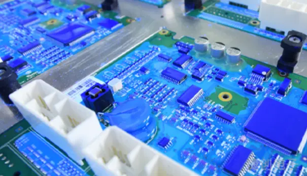 2. Switches and Push-Buttons
Tactile switches, DIP switches, and keypad switches contain movable contacts inside. When coating material penetrates the switch interior and cures, it can cause key sticking or failure of contacts to close. The masking coverage should include the switch body and its moving clearances.
3. Heat Sinks and Power Devices
Components such as MOSFETs, three-terminal voltage regulators, and power diodes often have heat sinks attached to their top surface or dissipate heat through a metal substrate. The thermal conductivity of conformal coating is significantly lower than that of metal, forming a thermal resistance layer that can cause component temperatures to exceed specifications. The masked area includes the heat sink surface and the interface between the component body and the heat sink.
4. Antenna Areas
The antenna areas of wireless modules such as Bluetooth, Wi-Fi, and GPS rely on an open electromagnetic field. The dielectric constant of the coating layer alters the antenna's resonant frequency and radiation efficiency, reducing communication range and sensitivity. The masked area covers the antenna trace region and the RF matching circuit.
5. Test Points and Programming Interfaces
ICT test points, programming pads, and debug interfaces are used for factory testing and firmware updates. The coating layer prevents probe contact, increasing test failure rates. The masked area includes all exposed metal test points and edge connectors.
6. High-Precision Sensors
MEMS sensors (accelerometers, gyroscopes), pressure sensors, humidity sensors, and similar devices rely on sensitive structures to respond to external physical quantities. The mass and stress introduced by the coating layer alter the sensor's zero point and sensitivity, introducing measurement errors. The masked area includes the sensor's vent holes and sensitive regions.
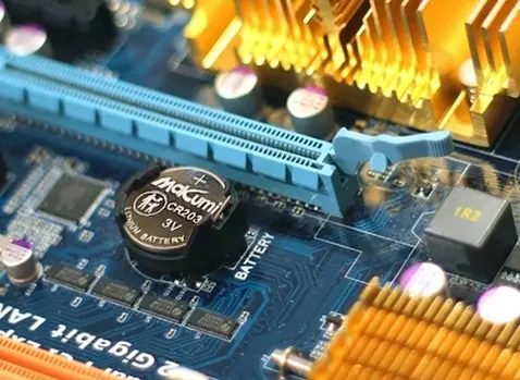
7. Battery Contacts and Spring Clips
Metal spring clips used to connect coin cells or rechargeable batteries must maintain low contact resistance. The coating layer forms an insulating film, causing power interruption to the device.
 Masking Implementation Recommendations
Use high-temperature resistant tape, peelable solder mask, or custom silicone fixtures for selective masking. After coating, remove the masking materials and inspect the boundaries for any leakage. For high-volume production, consider designing dedicated masking fixtures to improve consistency and efficiency.
Accurately identifying components that must not be coated is a fundamental step in ensuring PCBA reliability. In actual production, the masking strategy should be developed based on customer requirements and process standards.
With 17 years of expertise in PCBA design, manufacturing, and service, KingshengPCBA is ready to help turn your ideas into reality.
Feel free to contact us anytime to discuss your requirements and get a professional quotation.

 +86 13828766801
 kspcba@c-alley.com
 https://www.kingshengpcba.com/
 2/F, Building 6, Tangtou 3rd Industrial Zone, Tangtou Community, Shiyan Town, Baoan District, Shenzhen, China, 518108


