* On your first PCB Assembly order!
* Up to $300 discount
 C - A L L E Y
 Home | Events | PCB | About Us | News | Contact Us
Signal integrity remains one of the biggest challenges in high speed digital design. Among the many factors that affect signal quality, the return path—the often invisible route that current takes back to its source—is frequently underestimated. A poorly managed return path creates large loop areas that degrade timing, radiate electromagnetic interference, and compromise overall system reliability. For designers striving to meet the demands of modern electronics, minimizing return paths is not optional; it is essential.
I Why the Return Path Matters
Every signal forms a complete current loop: it leaves the driver, travels along the trace, passes through the receiver, and returns to the driver via the ground or power distribution system. The area enclosed by this loop directly determines: Loop inductance – larger loops increase inductance, slowing edge rates and reducing timing margins. EMI susceptibility and emission – the loop acts as an efficient antenna, both radiating noise and picking up external interference. Ground bounce – return currents flowing through shared impedance create voltage fluctuations that disturb multiple signals. Keeping this loop area as small as possible is the foundation of robust high speed layout.
II Practical Strategies for Return Path Control
1. Continuous Reference Planes
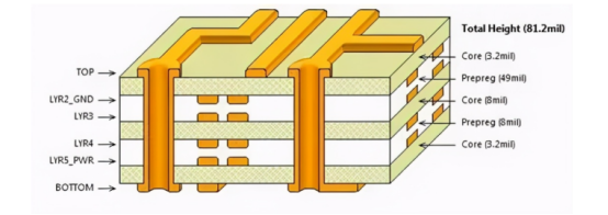
High speed signals must be routed over uninterrupted reference planes—preferably ground. Crossing splits in power or ground planes forces return currents to find a detour, drastically increasing the loop area. In a recent DDR4 design, address lines routed across a power plane split caused severe signal reflections. After the stack up was revised to place all critical signals directly over solid ground planes, timing margins passed validation.
2. Via Transitions with Return Vias
When a signal changes layers, its return current can lose its reference unless a nearby return via provides a continuous path. A best practice is to place a ground via adjacent to each signal via, with spacing no greater than 1/20 of the signal wavelength—for 10 Gbps signals, this is typically 30 mils or less. Precision manufacturing, including 6mil laser vias and 0.1 mm mechanical drilling, makes such fine pitched arrangements feasible.
3. Decoupling Capacitor Placement
High frequency return currents between power and ground planes rely on decoupling capacitors to complete the loop. Placing capacitors as close as possible to IC power pins, with direct via connections to the planes, minimizes the return path for high frequency noise. SMT assembly with 0201 component capability and placement accuracy of ±0.03 mm ensures that theoretical layouts become production reality.
4. Differential Pair Routing
For differential signals, the pair itself provides the primary return path. However, common mode noise still needs a clean ground reference. Maintaining tight intra pair skew (within 5 mils) and constant spacing prevents impedance mismatches that generate common mode energy and expand the effective loop area.
III How Advanced Manufacturing Enables Return Path Optimization
Even the most carefully designed return path strategy can fail if manufacturing capabilities cannot deliver the required precision. This is where a capable PCBA partner makes the difference.KING SHENG PCBA combines advanced fabrication with deep engineering support to ensure that return path designs are faithfully realized:
1. Layer registration is held to ±2 mils, preserving consistent impedance across via transitions and ensuring that signal layers remain aligned with their reference planes.
2. TDR impedance testing verifies that single ended 50 Ω and differential 100 Ω traces stay within ±10% tolerance—critical for maintaining controlled return paths.
3. Fine feature processing supports 2.5 mil trace/space, laser vias, and sequential lamination, giving designers the freedom to implement compact via arrangements and optimized stack ups.
4. DFM engineering review catches return path issues before production. Experienced engineers examine reference plane continuity, via placement, and decoupling capacitor layouts, helping customers avoid costly respins.
IV Conclusion
Minimizing return paths is a fundamental discipline in highspeed PCB design. When executed correctly, it preserves signal integrity, reduces EMI, and builds a foundation for reliable products. Translating these principles into physical hardware requires not only design skill but also a manufacturing partner capable of delivering the necessary precision and engineering insight.
KING SHENG PCBA provides that capability—combining ISO certified processes, advanced fabrication technology, and a team that understands the electrical implications of every manufacturing decision. For designers serious about signal integrity, having such a partner is the final, essential step in turning a well planned layout into a production ready success.
With 17 years of expertise in PCBA design, manufacturing, and service, KingshengPCBA is ready to help turn your ideas into reality. Feel free to contact us anytime to discuss your requirements and get a professional quotation.

Please send Email to kspcba@c-alley.com or call us through +86 13828766801 Or submit your inquiry by online form. Please fill out below form and attach your manufacturing files( PCB Gerber files and BOM List) if need quotation. We will contact you shortly.
 +86 13828766801
 kspcba@c-alley.com
 https://www.kingshengpcba.com/
 2/F, Building 6, Tangtou 3rd Industrial Zone, Tangtou Community, Shiyan Town, Baoan District, Shenzhen, China, 518108
We would also like to thank our customers for their trust and support. The company's outstanding achievements are mainly due to the loyalty of our customers, which also encourages and spurs our company to forge ahead.


