* On your first PCB Assembly order!
* Up to $300 discount
 C - A L L E Y
 Home | Events | PCB | About Us | News | Contact Us
In PCBA manufacturing, quality is non negotiable. A single undetected defect can lead to field failures, costly recalls, and reputation damage. That is why electrical testing – either In Circuit Test (ICT) or Flying Probe – is essential. But which one should you choose? The answer depends on your production volume, product maturity, and design complexity.
This article compares ICT and Flying Probe, and shows how a smart combination of both can maximize quality while minimizing cost.
I. ICT – The High Volume Workhorse
In Circuit Test (ICT) uses a custom “bed of nails” fixture. Hundreds of spring loaded probes contact dedicated test points on the PCB simultaneously. ICT performs fast, parallel measurements of shorts, opens, resistors, capacitors, and even some analog functions.
The main advantages of ICT are speed and low unit cost at scale. Testing takes only seconds to one minute per board, and fault coverage often exceeds 90% with precise component level diagnosis. However, ICT has significant downsides. The fixture itself costs several thousand US dollars per product and requires a lead time of two to four weeks. Any design change usually forces a new fixture. For small batches – typically below 500 to 1000 boards – the fixture cost per board becomes prohibitive.
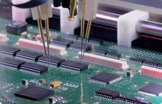
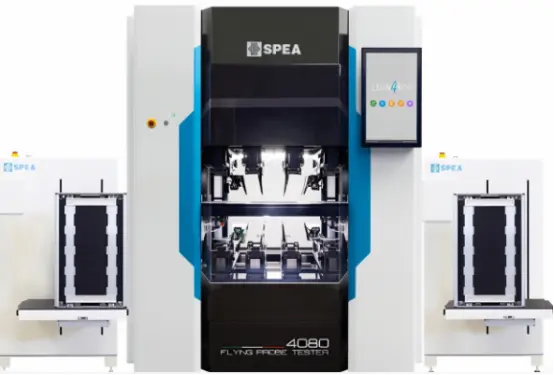
II. Flying Probe – The Agile Alternative
Flying Probe testers use two to eight moving probes driven by software. The probes “fly” across the board, touching test points or component pins one by one. No fixture is required at all. The key strengths of Flying Probe are zero fixture cost and fast program development – hours instead of days or weeks. The probes can reach fine pitch components with gaps as small as 0.2 mm, handling 01005 passives and high density designs easily. This makes Flying Probe ideal for prototypes, NPI (new product introduction), engineering validation, and rework verification. On the downside, Flying Probe is slow – typically three to fifteen minutes per board – and not suitable for high volume production lines. Fault coverage is also lower, usually between 70% and 85%, and more network level than component level.
III Head to Head without a Table
When comparing ICT and Flying Probe, several key differences stand out. ICT is extremely fast, testing a board in seconds, while Flying Probe takes minutes. ICT requires a costly, custom fixture; Flying Probe needs no fixture at all. ICT offers low flexibility – design changes mean a new fixture – whereas Flying Probe is highly flexible, needing only a software update. For PCB design, ICT demands dedicated test points with at least 0.5 mm pitch; Flying Probe can directly probe component pins. Fault coverage is above 90% for ICT versus 70 85% for Flying Probe. As a result, ICT is best suited for high volume mass production, while Flying Probe excels in prototypes, small batches, NPI, and rework.
IV The Winning Strategy: Combine Both
No single test method fits all situations. Smart PCBA factories use a hybrid approach. For NPI and small batches of fewer than 500 boards, Flying Probe is the first choice – no fixture investment and fast program changes when the design is revised. Once the product reaches stable high volume production, typically above 2000 boards, ICT becomes the main tester, delivering high throughput and low unit cost after fixture amortization. For rework verification and failure analysis, Flying Probe is again the better tool, as it can easily retest specific nets without building a new fixture. This combination typically reduces overall testing cost by about 30% while maintaining excellent quality.
V Special Case: High Density and High Reliability Products
For HDI boards, medical electronics, automotive modules, or 5G communication PCBs, traditional ICT may not have enough test point real estate. In these cases, Flying Probe is often the better choice – or a hybrid flow where Flying Probe covers dense areas and ICT handles the rest.
VI Why Partner with Us?
As a professional PCBA manufacturer, we offer both ICT and Flying Probe equipment in house, so we always match the test method to your project. We provide DFT (Design for Test) consulting to help you design testable PCBs from the start. Our fast program development reduces NPI cycle time, and our precise fault diagnosis and repair capabilities close the loop quickly – whether the defect is found by ICT or Flying Probe.
From ten prototype boards to one hundred thousand production units, we deliver reliable, cost optimized testing. Contact us to discuss the best test strategy for your next project.
With 17 years of expertise in PCBA design, manufacturing, and service, KingshengPCBA is ready to help turn your ideas into reality. Feel free to contact us anytime to discuss your requirements and get a professional quotation.

Please send Email to kspcba@c-alley.com or call us through +86 13828766801 Or submit your inquiry by online form. Please fill out below form and attach your manufacturing files( PCB Gerber files and BOM List) if need quotation. We will contact you shortly.
 +86 13828766801
 kspcba@c-alley.com
 https://www.kingshengpcba.com/
 2/F, Building 6, Tangtou 3rd Industrial Zone, Tangtou Community, Shiyan Town, Baoan District, Shenzhen, China, 518108
We would also like to thank our customers for their trust and support. The company's outstanding achievements are mainly due to the loyalty of our customers, which also encourages and spurs our company to forge ahead.


