* On your first PCB Assembly order!
* Up to $300 discount
 C - A L L E Y
 Home | Events | PCB | About Us | News | Contact Us
The acceleration of electronic product development places immense pressure on printed circuit board design. As the physical backbone of virtually every electronic system, the PCB must balance electrical performance, signal integrity, thermal behavior, and manufacturability—all within shrinking timelines.
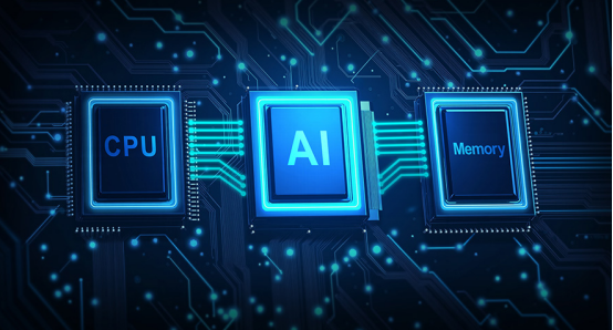
For decades, achieving this balance relied heavily on the manual expertise of layout engineers, a process that is both time-consuming and inherently variable. At KING SHENG PCBA, we are witnessing a paradigm shift: artificial intelligence is transforming PCB placement and routing from a rule based “does it connect?” exercise into a truly optimized, learning driven engineering discipline.
I The Limits of Traditional Approaches
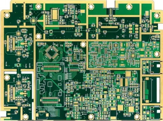
Conventional PCB design flows treat placement and routing as sequential, rule constrained tasks. Engineers place components based on experience, then use autorouters that follow predefined design rules (clearances, via counts, etc.). While these tools can achieve connectivity, they struggle with multi objective optimization—simultaneously minimizing signal interference, improving power integrity, simplifying manufacturing, and reducing cost. The result is often lengthy iterations, unpredictable design quality, and a disconnect between the design phase and the realities of high volume assembly.
II How AI Changes the Game
Modern AI techniques, particularly deep reinforcement learning and graph neural networks, turn PCB design into a holistic optimization problem. When trained on thousands of successful board layouts, AI models learn the hidden patterns of component interactions, signal flow, and thermal distribution. In the placement stage, AI can evaluate millions of arrangements in minutes, optimizing for total wire length, via count, routing congestion, and thermal uniformity—goals that are nearly impossible to balance manually.
For routing, reinforcement learning agents treat each net as a decision sequence. Unlike traditional autorouters that follow fixed heuristics, AI agents learn from trial runs to anticipate how local routing choices affect global routability. They can prioritize critical signals, avoid creating dead ends, and even adapt to complex mechanical constraints. The result is not just a routed board, but one that consistently meets electrical and manufacturing specifications with fewer passes.
III Design for Manufacturing
– Built In One of the most valuable aspects of AI driven layout is its natural alignment with Design for Manufacturing (DFM). AI systems can be trained on real production data—etching characteristics, solder paste behavior, assembly yields—so that they proactively avoid manufacturability pitfalls during the layout stage. Issues like acid traps, insufficient copper balance, or component placement that hinders automated optical inspection (AOI) are flagged and corrected before the design is released. This tight coupling of design and manufacturing data eliminates the traditional “over the wall” handoff and significantly reduces prototype spins.
IV KING SHENG PCBA: AI in Production
At KING SHENG PCBA, we have moved beyond theoretical discussions. We have integrated AI assisted layout tools into our engineering workflow, allowing our team to generate and evaluate multiple placement routing strategies in a fraction of the time previously required. For our customers, this means design cycles shortened by up to 60% and first pass prototype success rates exceeding 95%. Moreover, the output of AI enhanced design flows directly into our smart manufacturing platform. Placement coordinates, optimized panelization, and assembly aware routing data are fed seamlessly into our SMT lines, reflow profiling systems, and AOI equipment. This end toend digital continuity ensures that what is designed with AI can be manufactured with the highest consistency and yield.
V Looking Ahead
The next frontier is autonomous PCB design—where AI, given only a schematic and performance targets, can generate fully manufacturable layouts with minimal human intervention. Engineers will increasingly focus on defining design intent and validating AI generated results rather than performing manual routing. For manufacturing partners like KING SHENG, staying ahead requires not only adopting these AI tools but also continuously refining them with real world production data.
VI Conclusion
AI is not replacing the skilled PCB engineer; it is elevating the craft. By handling the complexity of multi objective optimization and manufacturability checks, AI frees engineers to concentrate on innovation. At KING SHENG PCBA, we are committed to harnessing this transformation—combining advanced AI assisted design with our deep manufacturing expertise—to deliver faster, more reliable, and more cost effective PCBA solutions. In an era where time to market is critical, intelligent layout and routing are no longer optional; they are the new standard. .
With 17 years of expertise in PCBA design, manufacturing, and service, KingshengPCBA is ready to help turn your ideas into reality. Feel free to contact us anytime to discuss your requirements and get a professional quotation.

Please send Email to kspcba@c-alley.com or call us through +86 13828766801 Or submit your inquiry by online form. Please fill out below form and attach your manufacturing files( PCB Gerber files and BOM List) if need quotation. We will contact you shortly.
 +86 13828766801
 kspcba@c-alley.com
 https://www.kingshengpcba.com/
 2/F, Building 6, Tangtou 3rd Industrial Zone, Tangtou Community, Shiyan Town, Baoan District, Shenzhen, China, 518108
We would also like to thank our customers for their trust and support. The company's outstanding achievements are mainly due to the loyalty of our customers, which also encourages and spurs our company to forge ahead.


