Methods to Avoid Bridging and Solder Icicles in Wave Soldering
 C - A L L E Y
Home | Events | PCB | About Us | News | Contact Us
In PCBA processing, wave soldering is a core step for soldering through-hole components. However, bridging and solder icicles are the two most common and troublesome defects in wave soldering. They not only affect the appearance of the board but can also lead to reliability issues such as short circuits or insufficient voltage withstand capability. Today, we will share several practical and effective control methods from a hands-on perspective.
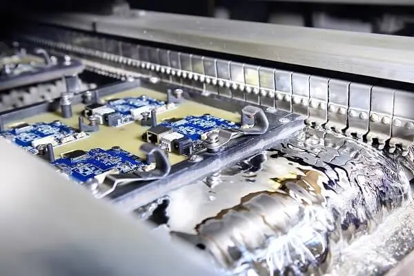 I. Root Causes of Bridging and Solder Icicles
Let's quickly identify the root causes:
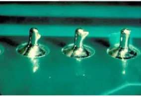
Bridging: Adjacent solder joints are abnormally connected by solder. This is common in areas with dense pin spacing. Main causes include insufficient flux activity, improper soldering angle, lack of solder thieves (or tear-drop pads), and poor solder fluidity.
Solder Icicles: The solder joint has a sharp, pointed protrusion. Typical causes include unreasonable PCB exit angle from the solder wave, low preheating temperature, insufficient soldering time, and increased impurity content in the solder pot.
 II. Six Practical Control Methods
1. Optimize Flux Spraying
II. Six Practical Control Methods
1. Optimize Flux Spraying
Flux is the "soul" of wave soldering. Insufficient or uneven spraying leads to abnormal solder surface tension, easily causing icicles and bridging.
- Recommend using a no-clean flux with moderate solid content, providing balanced activity and low residue.
- Regularly check the nozzle atomization effect to ensure even flux coverage on all pads.
- For high-density areas, slightly increase the spray amount, but avoid excessive residue on the board surface.
2. Adjust Preheating and Soldering Temperatures
The temperature profile determines solder wettability and fluidity.
- Preheating temperature is generally controlled at 90°C–120°C (measured on the board surface) to ensure full flux activation.
- Recommended solder pot temperature: 250°C–260°C for leaded solder, or 260°C–270°C for lead-free solder.
- Soldering time should be controlled between 2–5 seconds. Too long causes bridging; too short leads to icicles.
3. Adjust PCB Conveyor Angle and Direction
The angle affects solder drainage.
- Standard angle: 5°–7°. Too small an angle prevents solder from flowing back to the pot, causing bridging. Too large an angle reduces soldering time, leading to icicles.
- Conveyor direction: Align the long axis of component leads parallel to the conveyor direction as much as possible, avoiding lateral solder flow between dense pins.
4. Use Solder Thieves or Tear-Drop Pads
Solving the problem at the design stage is often the most thorough approach.
- Add dummy (non-functional) solder thieves at the end of dense connectors to guide excess solder away.
- For SOP, QFP, and similar through-hole components, design tear-drop pads or solder thieves at the end of each row of pins to effectively reduce bridging.
5. Check Wave Shape and Stability
An unstable wave is a "hidden killer" for bridging.
- Ensure the wave is level; the height difference between left and right should be less than 0.5 mm.
- A combination of turbulent wave + laminar wave is optimal: the turbulent wave eliminates shadowing effects, and the laminar wave completes solder drainage.
- Regularly remove dross to prevent oxidized particles from mixing into the solder flow and affecting fluidity.
6. Control Solder Impurities and Copper Content
Excessive copper content in lead-free solder significantly reduces fluidity, leading to icicles and bridging.
- Send solder samples for lab analysis every two weeks, keeping copper content below 0.8%.
- Periodically add pure solder or low-copper solder bars to dilute copper concentration.
- Maintain a stable solder pot level to avoid composition fluctuations caused by frequent material additions.
Conclusion
Bridging and solder icicles in wave soldering cannot be completely resolved by adjusting a single parameter. They require comprehensive optimization across six dimensions: flux, temperature, angle, wave shape, pad design, and solder composition. As a PCBA factory, it is recommended to establish a standardized wave soldering parameter checklist, record key parameters per shift, and regularly conduct Design of Experiments (DOE) to verify the optimal process window.
Shenzhen Kingsheng Technology Co., Ltd. has rich experience and a professional technical team in PCBA.
Contact KingshengPCBA today to request a quote or discuss your PCBA project.

 +86 13828766801
 kspcba@c-alley.com
 https://www.kingshengpcba.com/
 2/F, Building 6, Tangtou 3rd Industrial Zone, Tangtou Community, Shiyan Town, Baoan District, Shenzhen, China, 518108


