Key SMT Processes for High-Density Interconnect (HDI) Boards
 C - A L L E Y
Home | Events | PCB | About Us | News | Contact Us
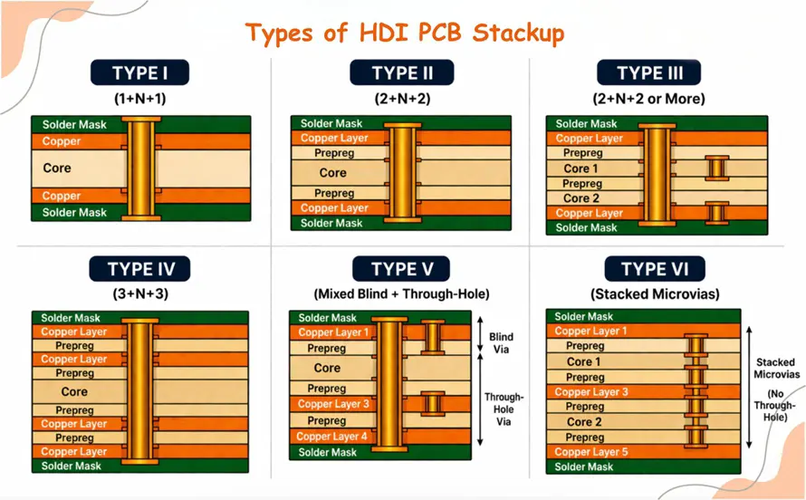
As electronic products evolve towards lighter, thinner, shorter, and higher-performance designs, High-Density Interconnect (HDI) boards have become the mainstream choice for smartphones, wearable devices, medical electronics, and automotive electronics. With line widths and spacings as fine as 50μm or even smaller, combined with complex blind vias, buried vias, and microvia structures, HDI boards present unprecedented challenges for Surface Mount Technology (SMT). For PCBA manufacturers, mastering the following key processes is essential to ensure the mounting quality and reliability of HDI boards.
 1. High-Precision Solder Paste Printing: The Starting Point of Yield
With HDI board pad pitches as small as 0.3mm or even 0.25mm, traditional stencils can no longer meet requirements. The key factors are:
Stencil Selection: Use electroformed or laser-cut + electro-polished stencils, with a recommended thickness of 0.08mm–0.10mm, aspect ratio ≥1.5, and area ratio ≥0.66.
Printing Parameters: Squeegee pressure, speed, and separation speed must be finely adjusted. Separation in particular should be "slow and steady" to avoid solder paste stringing or bridging.
Environmental Control: Strictly control temperature and humidity (25±3°C, 40%–60% RH) to prevent paste from drying and becoming sticky at fine pitches.
Recommendation: Perform SPI (Solder Paste Inspection) spot checks every 1–2 hours, with Cpk ≥1.33 as the target.
2. High-Precision Component Placement: The Art of Alignment and Stability
Given the small pad sizes and high density of HDI boards, placement machines must have:
High-Resolution Vision System: Use simultaneous top-and-bottom recognition with multi-stage lighting to ensure precise alignment of 01005 and even 008004 components.
Closed-Loop Placement Pressure Control: Prevent component shift or pad damage caused by local board warpage.
Substrate Support System: Use dedicated magnetic fixtures or vacuum suction platforms to prevent micro-vibrations of the HDI board during high-speed placement.
 3. Reflow Soldering: The Challenge of Temperature Difference Control
Due to multiple lamination structures, HDI boards have uneven copper distribution across different areas, resulting in significant thermal mass variation. Common issues include localized cold soldering or overheating leading to blind via cracking.
Oven Profile Optimization: Recommend using an RSS (Ramp-Soak-Spike) or RTS (Ramp-to-Spike) profile, with the key objective of controlling ΔT (maximum temperature difference across the board) to ≤10°C.
Nitrogen Protection: Fine-pitch solder joints are at high risk of oxidation. Keeping oxygen levels ≤1000ppm significantly improves wetting and reduces voids.
Microvia Outgassing: To address trapped voids at blind via bottoms, appropriately extend the preheat time (90–120s) to allow flux gas to escape.
4. Inspection and Rework: Invisible Defects Are the Greatest Risk
HDI board traces are highly concealed, and conventional AOI may not cover blind via bottoms and buried via areas.
3D X-Ray (CT Type): Essential for inspecting microvia solder quality beneath BGAs and CSPs, especially void rates and copper fill integrity.
Automated Optical Inspection (AOI): Must be equipped with a high-resolution camera (≥12 megapixels) and side-view lenses to capture abnormal solder joint shapes and fine bridging.
Rework Challenges: Thermal stress during HDI board rework can easily damage adjacent microvias. Use a small-diameter hot air nozzle (2mm larger than the component), strictly control heating time and temperature profiles, and consider laser-assisted heating when necessary.
Conclusion
The SMT process for high-density interconnect boards is not about optimizing a single step, but rather a system engineering effort integrating "solder paste printing – placement – reflow – inspection." The precision, stability, and process control capability of each step determine the final product's yield and long-term reliability. For PCBA manufacturers, investing in advanced inspection equipment and training operators in fine process discipline is far more cost-effective than post-hoc repair.
Shenzhen Kingsheng Technology Co., Ltd. has rich experience and a professional technical team in PCBA.
Contact KingshengPCBA today to request a quote or discuss your PCBA project.

 +86 13828766801
 kspcba@c-alley.com
 https://www.kingshengpcba.com/
 2/F, Building 6, Tangtou 3rd Industrial Zone, Tangtou Community, Shiyan Town, Baoan District, Shenzhen, China, 518108


