* On your first PCB Assembly order!
* Up to $300 discount
 C - A L L E Y
 Home | Events | PCB | About Us | News | Contact Us
In the PCBA manufacturing industry, the trend toward component miniaturization has never ceased. From the early days of 0805 and 0603, through the current mainstream 0201 and 0402, we are now entering the era of mass application of 01005 package components. Measuring just 0.4mm × 0.2mm × 0.2mm, the 01005 component has a volume less than one-tenth that of an 0402 component. For the placement process, this is not merely a matter of "getting smaller" — it marks the beginning of a series of systemic challenges.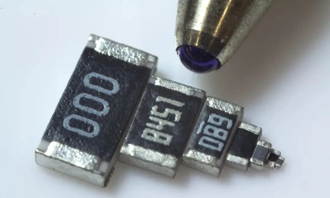
I. Precision Demands in Feeding and Pickup
The sprocket hole pitch of the tape for 01005 components remains the standard 4mm, but the relative clearance for the component within the pocket increases significantly. Vibrations generated by traditional pneumatic feeders during indexing can cause the component to stand on its side, flip over, or even jump out of the pocket. Our practical experience shows that an electric high-precision feeder is a basic requirement. Combined with an feeder cover equipped with static elimination, the pickup defect rate can be kept under control.
Nozzle selection is equally critical. The optimal nozzle inner diameter for 01005 components is between 0.12mm and 0.15mm, and the material should ideally be ceramic or tungsten steel with an anti-static coating. Rubber nozzles can cause positioning deviations due to slight deformation, while ordinary stainless steel nozzles tend to generate electrostatic attraction issues.
II. Breakthroughs in Vision Recognition
With a length and width of only 0.4mm × 0.2mm, 01005 components are easily affected by pad reflection and interference from adjacent components when using traditional down-looking cameras. We recommend using a combination of a multi-angle ring light and a high-resolution camera, along with a dedicated recognition algorithm for this component — reducing reliance on right-angle edges and instead using the grayscale gravity method for positioning.
Additionally, many factories overlook one detail: when the color contrast between the PCB's 01005 pad design and the solder mask is insufficient, the positioning error of the pad center as detected by the vision system is amplified. It is advisable to use "local Mark point compensation" in the placement program rather than relying solely on the global board reference.
III. Fine Control of Placement Pressure
Placement pressure is one of the most underestimated parameters in 01005 assembly. The 50g–80g placement pressure traditionally set for 0201 components is already too high for 01005 components. Excessive pressure can cause the component to fly off, squeeze solder paste and create shorts, or even damage the substrate pads.
The ideal range should be controlled between 30g and 50g, and the placement head must have real-time pressure feedback closed-loop control. Older equipment without pressure closed-loop is not recommended for mass production of 01005 components.
IV. Knock-on Challenges in Solder Paste Printing and Rework
The corresponding stencil aperture for 01005 components is typically around 0.22mm × 0.20mm, making it easy for the area ratio to fall below the industry empirical value of 0.66. Type 5 or higher-grade solder paste (powder diameter 15–25μm) must be used, and the stencil should ideally employ nano-coating or electroforming.
Rework is even more troublesome — if the hot air gun deviates even slightly, the component will be blown away. A dedicated small-scale rework station with a 0.3mm nozzle and a 20–40x microscope are essential tools.
Conclusion
01005 placement is not simply about increasing equipment precision by one notch; it is a comprehensive process upgrade covering feeding, recognition, placement pressure, printing, and rework. If your order already specifies 010005 components, be sure to verify each of the above aspects during the prototyping phase. If problems emerge only during mass production, the losses will far outweigh the upfront equipment investment.
Shenzhen Kingsheng Technology Co., Ltd. has rich experience and a professional technical team in PCBA. Contact KingshengPCBA today to request a quote or discuss your PCBA project.

Please send Email to kspcba@c-alley.com or call us through +86 13828766801 Or submit your inquiry by online form. Please fill out below form and attach your manufacturing files( PCB Gerber files and BOM List) if need quotation. We will contact you shortly.
 +86 13828766801
 kspcba@c-alley.com
 https://www.kingshengpcba.com/
 2/F, Building 6, Tangtou 3rd Industrial Zone, Tangtou Community, Shiyan Town, Baoan District, Shenzhen, China, 518108
We would also like to thank our customers for their trust and support. The company's outstanding achievements are mainly due to the loyalty of our customers, which also encourages and spurs our company to forge ahead.


