* On your first PCB Assembly order!
* Up to $300 discount
 C - A L L E Y
 Home | Events | PCB | About Us | News | Contact Us
Introduction
Micro-vias are a cornerstone of High-Density Interconnect (HDI) PCB technology, enabling compact, high-performance designs in modern electronics. UAnderstanding their size limitations is crucial for manufacturability, signal integrity, and reliability. This blog explores the minimum and maximum micro-via sizes, industry standards, design considerations, and emerging trends.
I. Defining Micro-Vias
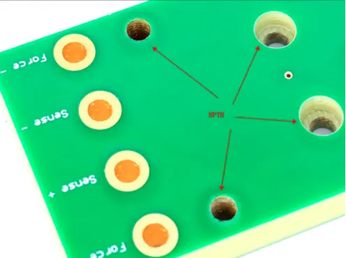
Micro-vias are small, laser-drilled holes (typically ≤150µm in diameter) used to connect different layers in HDI PCBs. They are categorized into: 1.Blind vias (connect outer to inner layers). 2.Buried vias (connect inner layers only). 3.Stacked or staggered vias (for high-density routing).
II. Minimum Micro-Via Size: How Small Can You Go?
Industry Standards & Practical Limits The smallest achievable micro-via size depends on fabrication technology, materials, and design requirements:
Key Constraints:
1.Laser Drilling Precision: CO₂/UV lasers can achieve ~25µm holes but require ultra-thin dielectrics.
2.Material Limitations: Polyimide or FR-4 must withstand drilling without delamination.
3.Plating Challenges: Smaller vias risk incomplete copper deposition, leading to reliability issues.
Example Applications:
4.Consumer Electronics (smartphones, wearables) often use 50–75µm micro-vias.
5.Medical Implants may push limits to 25–40µm for ultra-miniaturization.
III. Maximum Micro-Via Size: When Bigger is Better
Upper Limits & Design Trade-offs
While micro-vias are defined as ≤150µm, designers sometimes use larger "transitional" vias (150–300µm) for:
1.Higher Current Carrying Capacity (e.g., power delivery networks).
2.Easier Manufacturability (reduced plating defects).
3.Thermal Management (better heat dissipation).
Practical Considerations:
1.IPC-2226 Standards: Classifies vias >150µm as "standard" rather than "micro."
2.Flex PCBs: Larger vias (up to 200µm) improve mechanical stability in bend areas.
IV. Critical Design Factors Beyond Size
Aspect Ratio & Reliability
1.Optimal Aspect Ratio: 0.8:1 (e.g., 80µm hole depth for a 100µm diameter via). Higher ratios risk plating voids.
2.Stacked vs. Staggered Vias: Stacked micro-vias require tighter process control to avoid stress fractures.
Material Selection
1.Low-CTE Dielectrics (e.g., Megtron 6) reduce thermal stress on small vias.
2.Flexible Substrates: Polyimide demands larger vias (≥75µm) for durability.
Manufacturing Tolerances
1.Laser Drilling Tolerance: ±10–15µm for diameters <100µm.
2.Copper Plating: Minimum 15µm wall thickness for reliability. V. Future Trends: Pushing the Boundaries 1.Sub-20µm Vias: Research into photolithography and additive manufacturing for next-gen IC substrates. 2.3D Printed Electronics: Potential to create non-cylindrical via geometries.
3.A.I.-Optimized Designs: Machine learning to balance size, density, and signal integrity
Conclusion: Balancing Size with Functionality
The minimum micro-via size is ~25–50µm for cutting-edge HDI, while the maximum typically aligns with the 150µm micro-via threshold. Designers must weigh:
1.Performance Needs (signal integrity, current load).
2.Fabrication Capabilities (laser drilling, plating).
3.Cost vs. Complexity (smaller vias increase production costs).
Pro Tip: Collaborate early with your PCB manufacturer to validate via designs for yield and reliability.
With 17 years of expertise in PCBA design, manufacturing, and service, KingshengPCBA is ready to help turn your ideas into reality. Feel free to contact us anytime to discuss your requirements and get a professional quotation.

Please send Email to kspcba@c-alley.com or call us through +86 13828766801 Or submit your inquiry by online form. Please fill out below form and attach your manufacturing files( PCB Gerber files and BOM List) if need quotation. We will contact you shortly.
 +86 13828766801
 kspcba@c-alley.com
 https://www.kingshengpcba.com/
 2/F, Building 6, Tangtou 3rd Industrial Zone, Tangtou Community, Shiyan Town, Baoan District, Shenzhen, China, 518108
We would also like to thank our customers for their trust and support. The company's outstanding achievements are mainly due to the loyalty of our customers, which also encourages and spurs our company to forge ahead.


