* On your first PCB Assembly order!
* Up to $300 discount
 C - A L L E Y
 Home | Events | PCB | About Us | News | Contact Us
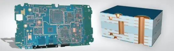
In the ever-shrinking world of electronics, micro-vias have become a cornerstone of high-density interconnect (HDI) printed circuit boards (PCBs). These tiny conduits enable the multilayer routing essential for today’s compact, high-performance devices—from smartphones to medical implants. But what exactly are they, and why do they matter? Let’s dive in.
I. Definition & Structure
A micro-via is a miniature conductive hole (typically ≤150µm in diameter) that connects layers in a multilayer PCB. Unlike traditional through-hole vias,
micro-vias are:
1.Blind or Buried: They span between adjacent layers (blind) or internal layers (buried), not the entire board.
2.Laser-Drilled: Precision lasers create these ultra-small holes, enabling finer pitches and higher density.
3.Filled/Plated: Often filled with conductive material (e.g., copper) to ensure reliable interlayer connections. A micro via is a tiny hole drilled in a PCB that connects different layers of the board. Unlike standard vias, micro vias are significantly smaller, typically measuring less than 150 micrometers (μm) in diameter. These miniature connections play a vital role in creating more compact and efficient circuit designs, particularly in HDI boards.
II: Key Characteristics of Micro Vias
1.Diameter: Usually less than 150 μm
2.Aspect ratio: Typically 1:1 or less
3.Depth: Often limited to connecting adjacent layers
4.Manufacturing method: Laser drilling or photo-defined processes
Micro vias have revolutionized PCB design by allowing for higher component density and improved signal integrity, making them indispensable in modern electronics manufacturing.
III : Why Micro-Vias? Key Advantages
1.Space Efficiency
2.Micro-vias allow designers to pack more circuitry into smaller areas, critical for wearables and IoT devices.
3.Enhanced Signal Integrity
4.Shorter vertical paths reduce parasitic capacitance/inductance, improving high-frequency performance (e.g., 5G, RF applications).
5.Design Flexibility
6.Enable complex HDI layouts, including stacked (multiple micro-vias atop each other) and staggered configurations.
Ⅳ. Manufacturing Challenges & Solutions
While indispensable, micro-vias demand advanced processes:
1.Laser Precision: CO₂ or UV lasers must drill without damaging surrounding materials.
2.Plating Uniformity: Electroplating tiny holes requires specialized chemistry to avoid voids.
3.Thermal Reliability: Repeated thermal cycling (e.g., in automotive PCBs) risks cracks—filled vias mitigate this.
V. Applications: Where Micro-Vias Shine
1.Consumer Electronics: Smartphones (e.g., Apple’s A-series chips use micro-vias).
2.Medical Devices: Implantable sensors requiring ultra-miniaturization.
3.Aerospace: Lightweight, high-reliability avionics.
VI. Future Trends
As devices push toward 3D-IC packaging and sub-µm features, micro-vias will evolve with:
1.Advanced Materials: Low-loss dielectrics for higher frequencies.
2.Hybrid Designs: Combining micro-vias with through-silicon vias (TSVs).
Conclusion
Micro-vias are the unsung heroes of modern electronics, enabling the sleek, powerful gadgets we rely on daily. For OEMs and designers, partnering with a PCBA manufacturer skilled in HDI processes (like laser drilling and via filling) is crucial to harnessing their full potential.
Need micro-via expertise for your next project?
Contact C-alley for cutting-edge PCB solutions.
With 17 years of expertise in PCBA design, manufacturing, and service, KingshengPCBA is ready to help turn your ideas into reality. Feel free to contact us anytime to discuss your requirements and get a professional quotation.

Please send Email to kspcba@c-alley.com or call us through +86 13828766801 Or submit your inquiry by online form. Please fill out below form and attach your manufacturing files( PCB Gerber files and BOM List) if need quotation. We will contact you shortly.
 +86 13828766801
 kspcba@c-alley.com
 https://www.kingshengpcba.com/
 2/F, Building 6, Tangtou 3rd Industrial Zone, Tangtou Community, Shiyan Town, Baoan District, Shenzhen, China, 518108
We would also like to thank our customers for their trust and support. The company's outstanding achievements are mainly due to the loyalty of our customers, which also encourages and spurs our company to forge ahead.


