* On your first PCB Assembly order!
* Up to $300 discount
 C - A L L E Y
 Home | Events | PCB | About Us | News | Contact Us
In the race to build smaller, faster, and more powerful electronics, HDI (High-Density Interconnect) technology has emerged as a game-changer. From smartphones to aerospace systems, HDI PCBs enable the intricate circuitry that powers modern innovation. But what exactly does HDI mean, and why is it revolutionizing electronics manufacturing? This deep dive explores its definition, benefits, manufacturing nuances, and future trends.
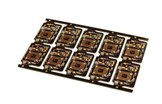
I. HDI Defined: Beyond the Acronym
HDI stands for High-Density Interconnect, a PCB design and manufacturing approach that maximizes component density and minimizes space usage.
Key hallmarks include:
1.Micro-Vias: Laser-drilled holes (≤150µm) connecting adjacent layers, enabling tighter routing.
2.Fine-Pitch Components: Supports smaller traces/spaces (e.g., 40µm/40µm vs. 100µm/100µm in traditional PCBs).
3.Sequential Lamination: Multiple lamination cycles to build ultra-thin, multilayer stacks. Example: A smartphone motherboard uses HDI to fit 10+ layers into a 1mm thickness, versus 2mm+ with conventional methods.
II. Why HDI? The Competitive Edge
1.Miniaturization: Shrinks PCB footprint by 30–50%, critical for wearables and IoT devices. Enables any-layer via designs (e.g., Apple’s A-series chips).
2.Performance Boost: Shorter signal paths reduce latency and EMI, ideal for 5G and high-speed data (e.g., DDR5 memory). Improved thermal management via optimized copper distribution.
3.Reliability :Fewer mechanical through-holes lower failure risks (e.g., thermal stress cracks). Advanced materials (e.g., low-loss dielectrics) enhance longevity.
III. HDI Manufacturing: Precision Meets Complexity
Producing HDI PCBs demands cutting-edge techniques:
1. Laser Drilling CO₂/UV lasers create micro-vias with ±10µm accuracy. Challenge: Avoiding residue buildup (solved via plasma cleaning).
2. Sequential Lamination :Layers are bonded incrementally to prevent misalignment. Key Step: Via filling with conductive paste ensures planar surfaces for further layering.
3. Advanced Imaging: LDI (Laser Direct Imaging) replaces photomasks for finer traces (≤20µm). Data Point: HDI yields drop by ~15% versus standard PCBs due to process complexity—highlighting the need for expert manufacturers.
V. Real-World Applications of HDI
1.Consumer Electronics: iPhone’s stacked HDI design integrates 12+ layers in 0.8mm.
2.Medical: Implantable defibrillators use HDI for reliability in life-critical systems.
3.Automotive: ADAS (Advanced Driver Assistance Systems) rely on HDI for compact, high-speed sensor arrays.
VI: The Future of HDI: What’s Next?
1. 3D Integration: Combining HDI with TSVs (Through-Silicon Vias) for 3D-IC packaging. Example: NVIDIA’s H100 GPU uses hybrid HDI/TSV interconnects.
2. Material Innovations: Ultra-Low-Loss Dielectrics: For terahertz-frequency applications (e.g., 6G). Flexible HDI: Bendable PCBs for foldable phones (e.g., Samsung Galaxy Z Fold).
3. Sustainability: Lead-free via fill materials and recyclable substrates to meet EU RoHS 3.0 standards.
Conclusion: HDI as the Backbone of Innovation
HDI isn’t just an acronym—it’s the foundation of tomorrow’s electronics. As devices demand higher performance in smaller form factors, partnering with an HDI-savvy PCBA manufacturer becomes strategic. From design support (e.g., DFM checks) to advanced processes like laser drilling, the right collaborator ensures your boards meet cutting-edge specs.
Ready to leverage HDI for your next project? Contact C-alley for end-to-end HDI solutions—from prototyping to mass production .
With 17 years of expertise in PCBA design, manufacturing, and service, KingshengPCBA is ready to help turn your ideas into reality. Feel free to contact us anytime to discuss your requirements and get a professional quotation.

Please send Email to kspcba@c-alley.com or call us through +86 13828766801 Or submit your inquiry by online form. Please fill out below form and attach your manufacturing files( PCB Gerber files and BOM List) if need quotation. We will contact you shortly.
 +86 13828766801
 kspcba@c-alley.com
 https://www.kingshengpcba.com/
 2/F, Building 6, Tangtou 3rd Industrial Zone, Tangtou Community, Shiyan Town, Baoan District, Shenzhen, China, 518108
We would also like to thank our customers for their trust and support. The company's outstanding achievements are mainly due to the loyalty of our customers, which also encourages and spurs our company to forge ahead.


