* On your first PCB Assembly order!
* Up to $300 discount
 C - A L L E Y
 Home | Events | PCB | About Us | News | Contact Us
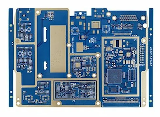
Look at any modern electronic device—a sleek smartphone, a tiny fitness tracker, or a life-saving medical implant. What strikes you first is how small, powerful, and beautiful these devices have become. Behind this transformation lies an unsung hero: the printed circuit board.
Over the past decades, PCBs have evolved from humble single-sided boards to sophisticated High-Density Interconnect (HDI) masterpieces. This journey from "simple and functional" to "small and beautiful" has enabled the electronic revolution we now take for granted.
At Shenzhen Kingsheng Tech Co., Ltd. , with over 22 years of specialized PCB manufacturing experience serving clients in Australia, the United States, Italy, and across Europe, we have witnessed and contributed to this remarkable evolution. Here's the story of how PCBs learned to shrink without compromising performance.
Chapter 1: The Humble Beginning – Single-Sided PCBs
In the early days of electronics, PCBs were simple. A single-sided board had copper traces on just one side of an insulating substrate. Components were mounted on the opposite side, with holes drilled through for leads to connect.
Characteristics:
Single-sided PCBs served their purpose well for radios, calculators, and early consumer electronics. But as devices became more sophisticated, their limitations became clear: you simply couldn't pack enough functionality into a small space.
Chapter 2: The First Leap – Double-Sided and Multi-Layer
The next logical step was putting copper on both sides of the board. Double-sided PCBs doubled the available routing area without increasing board size. Then came multi-layer boards—stacking multiple copper layers separated by insulating material.
The Breakthrough: Plated Through-Holes (PTH)
The real magic happened with plated through-holes. By electroplating copper inside drilled holes, manufacturers could connect different layers electrically. This simple innovation unlocked the potential for truly complex designs.
Double-Sided PCB Characteristics:
Multi-Layer PCB Characteristics:
Chapter 3: The Miniaturization Challenge
As consumer devices shrank, PCB technology had to keep pace. The challenges were formidable:
More functionality in less space: Smartphones needed to pack computing power, wireless connectivity, cameras, and sensors into increasingly thin profiles
Traditional multi-layer PCBs hit physical limits. Drilled holes took up space, and routing density maxed out. Something new was needed.
Chapter 4: The "Beautiful" Part – How HDI Enables Modern Design
The shift to HDI isn't just about making things smaller—it's about making them better. Here's how HDI contributes to the "beautiful" in modern electronics:
1. Thin and Light
HDI boards can be significantly thinner than conventional multi-layer boards. For smartphones and wearables, every millimeter matters. An HDI board with the same functionality as an 8-layer conventional board might be 30-40% thinner.
2. More Functionality
With higher routing density, HDI boards pack more features into the same space. A modern smartphone PCB might include:
All in a board smaller than a credit card
3. Better Signal Integrity
For high-speed applications like 5G and AI processors, this is essential.
4. Thermal Management
More layers and better via structures allow for improved heat dissipation. Thermal vias can channel heat away from hot components, keeping devices cool in thin enclosures.
5. Design Freedom
HDI technology enables creative industrial design:
Why Shenzhen Kingsheng Tech for Your HDI Journey
At Shenzhen Kingsheng Tech, our 22 years of PCB manufacturing experience have prepared us for the HDI revolution. We offer:
Quality Assurance
Engineering Support
Global Experience
Conclusion: Small, Beautiful, and Reliable
The evolution from single-sided boards to HDI technology represents one of electronics' greatest achievements. What was once a simple platform for connections has become an engineered marvel enabling the devices we love.
At Shenzhen Kingsheng Tech, we're proud to have participated in this journey for over two decades. Whether you need a simple prototype or a complex HDI design for your next innovation, we have the experience and capabilities to bring your vision to life.
Ready to make your next product smaller, smarter, and more beautiful?
Contact Shenzhen Kingsheng Tech today to discuss how our HDI expertise can help you achieve the miniaturization your design deserves.
With 16 years of expertise in PCBA design, manufacturing, and service, KingshengPCBA is ready to help turn your ideas into reality. Feel free to contact us anytime to discuss your requirements and get a professional quotation.

Please send Email to kspcba@c-alley.com or call us through +86 13828766801 Or submit your inquiry by online form. Please fill out below form and attach your manufacturing files( PCB Gerber files and BOM List) if need quotation. We will contact you shortly.
 +86 13828766801
 kspcba@c-alley.com
 https://www.kingshengpcba.com/
 2/F, Building 6, Tangtou 3rd Industrial Zone, Tangtou Community, Shiyan Town, Baoan District, Shenzhen, China, 518108
We would also like to thank our customers for their trust and support. The company's outstanding achievements are mainly due to the loyalty of our customers, which also encourages and spurs our company to forge ahead.


