* On your first PCB Assembly order!
* Up to $300 discount
 C - A L L E Y
 Home | Events | PCB | About Us | News | Contact Us
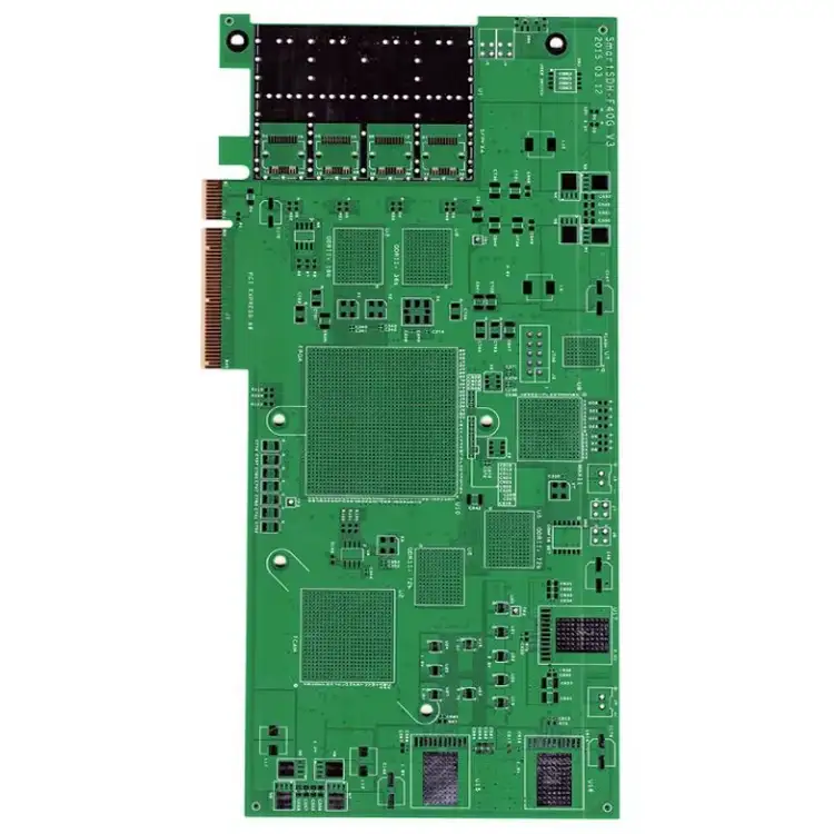
In the field of electronics manufacturing, the manufacturability of PCBA design directly determines whether a product can be produced efficiently and to a high standard. Many hardware engineers focus too heavily on electrical performance during the design phase, whilst overlooking the practical constraints of the manufacturing process. This often leads to frequent issues during pilot production, such as components that cannot be mounted, high rates of soldering defects, and incomplete test coverage.
The root cause of these problems usually lies in insufficient consideration of manufacturability during the design phase.
Paying attention to key points from the design stage onwards is crucial to achieving good manufacturability. This article will systematically outline the core principles of PCBA design for manufacturability, helping engineers to pave the way for subsequent manufacturing right from the design stage, thereby shortening time-to-market and reducing manufacturing costs.
I. Considerations regarding the rationality of circuit design
Signal Integrity Design:
When designing circuits, signal integrity must be given the utmost attention. For high-speed signal lines, their length should be kept as short as possible, and the number of vias minimised. Taking the PCBA of a high-speed data transmission device as an example, excessively long high-speed signal lines can easily lead to signal attenuation, delay and reflection, thereby affecting the accuracy of data transmission. By carefully planning the layout and positioning the high-speed signal source as close as possible to the receiver, signal transmission losses can be effectively reduced.
At the same time, controlling the size and spacing of vias, and selecting appropriate via types (such as blind vias or buried vias), can minimise signal interference at the via locations. For differential signals, it is essential to ensure that the two lines within the differential pair are of equal length and maintain equal spacing to prevent the generation of common-mode noise. These design details ultimately determine the transmission quality of high-speed signals.
High-frequency signal lines require impedance control, such as 50Ω for single-ended signals and 100Ω for differential signals, which is achieved by adjusting line width, spacing and dielectric thickness. The precision of impedance control directly affects signal reflection loss; for high-speed signals at the Gbps level, impedance deviation must be kept within ±10%.
Optimisation of Power Distribution Systems:
The design of the power distribution system has a significant impact on manufacturability. It is essential to ensure that the power plane layout is rational, avoiding the formation of power islands or areas with excessive voltage drops. When designing PCB assemblies for multi-chip systems, as different chips have varying power requirements, the power and ground planes must be planned appropriately based on the chips’ power consumption and distribution.
When using multi-layer PCBs, power planes and signal layers should be allocated appropriately. Measures such as increasing the copper foil thickness of the power planes and optimising power routing can reduce power resistance and enhance the stability of power distribution. Power planes and ground planes should be arranged in parallel to minimise power supply noise; high-current paths require wider copper traces or the use of multiple vias in parallel. This not only meets the power requirements of the chips but also facilitates power supply debugging and testing during the manufacturing process, thereby reducing manufacturing challenges caused by power supply issues.
II. Key Considerations for Component Selection and Layout
Compatibility and versatility in component selection:
During the component selection phase, priority should be given to components that offer good compatibility and versatility. Avoid selecting components that are too specialised or niche, to prevent issues such as procurement difficulties, excessive costs or incompatibility with other components during the manufacturing process.
For instance, when selecting basic components such as resistors and capacitors, give priority to products with industry-standard packaging and specifications, such as the commonly used 0402 and 0603 packages. These components are readily available on the market, offer stable pricing, and are easy to solder and test. For integrated circuit chips, consider their compatibility with the surrounding circuitry, as well as the availability of reliable suppliers and technical support, to ensure they can be readily obtained and utilised during the manufacturing process.
For products requiring long-term storage, it is recommended to select components with ENIG (electroless nickel-gold) surface treatment to avoid bridging in fine-pitch components caused by the uneven surface of HASL (hot air solder levelling). For high-frequency applications, materials with low dielectric constants (such as Rogers 4350B) should be selected to reduce signal loss.
The rationality of component layout:
Component layout should take full account of manufacturing process requirements. In SMT processing, sufficient spacing must be maintained between components to facilitate the placement and removal of components by the pick-and-place machine’s nozzle, as well as the soldering operation. For micro-package components such as 0402 and 0201, spacing must be strictly controlled within a certain range to ensure the quality of solder paste printing and soldering. It is generally recommended that the spacing between micro-components be no less than 0.3 mm to facilitate AOI inspection and rework operations.
High-heat-generating components should be distributed rationally, with sufficient space reserved for heat dissipation to prevent heat concentration from affecting the performance of other components. High-power devices must be positioned close to heat dissipation channels or with space reserved for heat sink installation. During the DIP insertion stage, ensure that the orientation and positioning of the component leads facilitate insertion and soldering by operators, avoiding lead interference or insufficient working space.
The layout must also take into account the design of test points. Sufficient test points must be provided for ICT testing to ensure probe contact. Test points should be evenly distributed to avoid excessive concentration, which could complicate fixture fabrication. For BGA devices, test vias must be provided around the periphery to facilitate signal measurement.
III. Adapting PCB Design to Manufacturing Processes
Number of PCB Layers and Board Selection:
The choice of PCB layer count and substrate material must take into account both product performance and manufacturing costs. For simple products with modest electrical performance requirements, PCBs with fewer layers—such as double-sided or four-layer boards—may be selected to reduce manufacturing costs. Conversely, for products involving high-frequency and high-speed signal transmission, such as PCB assemblies for 5G communication equipment, multi-layer PCBs and high-performance substrates may be required to meet the demands for low signal loss and high stability.
In high-power applications (such as LED drivers and power supply modules), metal substrates (aluminium substrates) or thick copper foil (≥2 oz) must be used to enhance heat dissipation. For flexible circuits (FPCs), polyimide (PI) substrates should be selected, as they are resistant to bending and high temperatures. Furthermore, the appropriate number of PCB layers and substrate materials must be chosen based on the manufacturer’s process capabilities to ensure the feasibility of the manufacturing process and consistent quality.
PCB Circuit and Via Design:
The width and spacing of PCB traces must comply with manufacturing process requirements. Generally speaking, trace width should be determined based on current-carrying capacity and manufacturing precision; for example, for power lines carrying higher currents, the trace width should be increased appropriately to reduce trace resistance. Trace spacing must take into account the prevention of short circuits and etching precision during the manufacturing process, to avoid short circuits or etching difficulties caused by excessively small spacing.
Via design is also of critical importance. The size, quantity and distribution of vias should be optimised according to electrical connection requirements and manufacturing processes. For high-density PCBs, microvia technology may be employed to increase via density and improve routing efficiency, whilst ensuring machining precision and reliability. High-speed signal vias require back drilling to reduce parasitic capacitance; the number of power/ground vias should be increased to lower impedance.
Pad design is equally important. Pad dimensions must be matched to the component package type to prevent cold solder joints or bridging; for BGA pads, the differences between via-cut and non-via-cut areas in the solder mask must be taken into account. For QFN devices, the design of the heat sink pad directly affects heat dissipation and must ensure a good connection to the ground plane.
Screen printing and branding:
Although silkscreen markings may seem like a minor detail, they actually have a significant impact on production efficiency and serviceability. Component part numbers and polarity markings must be clear and should not overlap with pads. Test points must be provided in the BGA area to facilitate fault diagnosis. Silkscreen characters must be heat-resistant (≥260°C) to prevent blurring after reflow soldering. For components requiring manual insertion, polarity markings should be clearly visible to minimise the risk of incorrect insertion.
IV. The Importance of DFM Review
DFM (Design for Manufacturability) reviews serve as a bridge between design and manufacturing. Professional PCBA factories offer DFM services, getting involved in the review process during the design stage to help clients identify potential issues. The review covers aspects such as whether trace spacing meets minimum requirements, whether hole diameters comply with drill specifications, whether component placement facilitates assembly, and whether there are sufficient test points.
Through DFM reviews, designs can be modified prior to production, thereby preventing batch defects. A case involving a smart wearable device manufacturer, where a 0.1mm deviation in trace width led to short circuits across an entire batch, highlights the critical importance of design reviews. For complex BGA and QFN packages, DFM reviews can also help optimise pad design and improve soldering yield.
Conclusion
The core of Design for Manufacturability (DFM) in PCBA lies in striking the optimal balance between electrical performance and manufacturing processes. The rationality of the circuit design, the versatility of component selection, the process adaptability of the layout, and the cost-effectiveness of board selection—these factors are intertwined and collectively determine whether a product can successfully progress from the drawing board to a physical prototype.
For hardware engineers, mastering the methodology of Design for Manufacturability (DFM) not only shortens product development cycles but also reduces manufacturing costs and enhances product quality. Selecting manufacturing partners with DFM capabilities and incorporating a process perspective from the design stage is an effective approach to achieving high-quality PCBA manufacturing.
With 16 years of expertise in PCBA design, manufacturing, and service, KingshengPCBA is ready to help turn your ideas into reality. Feel free to contact us anytime to discuss your requirements and get a professional quotation.

Please send Email to kspcba@c-alley.com or call us through +86 13828766801 Or submit your inquiry by online form. Please fill out below form and attach your manufacturing files( PCB Gerber files and BOM List) if need quotation. We will contact you shortly.
 +86 13828766801
 kspcba@c-alley.com
 https://www.kingshengpcba.com/
 2/F, Building 6, Tangtou 3rd Industrial Zone, Tangtou Community, Shiyan Town, Baoan District, Shenzhen, China, 518108
We would also like to thank our customers for their trust and support. The company's outstanding achievements are mainly due to the loyalty of our customers, which also encourages and spurs our company to forge ahead.


