* On your first PCB Assembly order!
* Up to $300 discount
 C - A L L E Y
 Home | Events | PCB | About Us | News | Contact Us
Behind what appears to be a simple PCBA (Printed Circuit Board Assembly) lies a process comprising dozens of precision operations. From the engineer’s initial design concept to the final functional implementation, every stage requires rigorous process control and quality management. In the case of electronic products, the quality of the PCBA directly determines the performance and lifespan of the entire device. This article provides an in-depth analysis of the entire PCBA manufacturing process, revealing the 11 key steps involved from design to finished product, to help readers gain a comprehensive understanding of this complex manufacturing process.
Ⅰ: Design Verification and Preparation
1: Design for Manufacturing (DFM) review
The first stage of PCBA manufacturing begins with a rigorous review of the design documents. The engineering team first conducts a manufacturability analysis of the Gerber files, BOMs and coordinate files to ensure that parameters such as trace spacing and hole diameters meet production process requirements. This seemingly simple check is, in fact, key to avoiding ‘inherent defects’.
A real-life case serves as a stark warning: a manufacturer of smart wearable devices once suffered short circuits across an entire batch of products due to overlooking a 0.1mm deviation in line width, resulting in losses amounting to several million yuan. The significance of DFM checks lies precisely in nipping problems in the bud. For special packaging components such as BGAs and QFNs, engineers must also pay particular attention to whether the pad designs are compatible and whether the solder mask opening patterns are appropriate. Neglecting these details can trigger a chain reaction in subsequent manufacturing stages.
2: Process Planning
Once the DFM review has been completed, process engineers must develop appropriate soldering processes based on the characteristics of the components. For example, automotive electronic PCBs often require a triple-coat protective varnish process to withstand harsh operating conditions; whereas for mixed-assembly boards (SMT + THT), the SMT process must be completed first, followed by the THT process, to avoid damage to components caused by repeated exposure to high temperatures.
Another key aspect of process planning is determining the stencil design. The stencil thickness must match the component lead pitch—QFP components with a 0.4 mm pitch typically require a 0.12 mm thick stencil. Parameters such as printing pressure and de-moulding speed must also be pre-set to ensure that the solder paste is accurately transferred onto the pads.
Ⅱ: Core manufacturing processes
3: Solder paste printing
Solder paste printing is the first step in SMT production and a critical stage that determines the quality of the solder joints. Solder paste is precisely printed onto the pad locations using a laser-cut stencil; modern production lines are typically equipped with 3D SPI inspection systems to monitor solder paste thickness and shape in real time. Data indicates that approximately 70% of soldering defects stem from poor solder paste printing, making SPI an indispensable quality control point.
The process window for solder paste printing is relatively narrow: printing pressure must be controlled between 0.1 and 0.3 N/mm² to prevent the solder paste from collapsing or missing the pad; component placement must be completed within one hour of printing to prevent oxidation of the solder paste. For fine-pitch components, the stencil aperture design must also take into account the aspect ratio and area ratio to ensure the solder paste is dispensed smoothly.
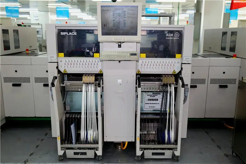
4: Surface Mount Technology (SMT)
High-speed placement machines are the core equipment of SMT production lines. Modern placement machines place components at a rate of tens of thousands per hour; for micro-package components such as 0402 and 0201, a vision alignment system must be employed to ensure placement accuracy. Polarised components such as LEDs and electrolytic capacitors also require special orientation calibration procedures to prevent functional failure caused by incorrect orientation.
The precision of the placement machine directly impacts soldering quality. The equipment must be calibrated daily upon start-up to ensure component offset is ≤±0.05mm. As a consumable part, the nozzle must be replaced regularly (e.g. every 5,000 placements) to prevent component rejection caused by wear. Such meticulous management ultimately results in consistently stable production yield.
5: Reflow soldering
Reflow soldering is at the heart of the SMT process, and the configuration of its temperature profile directly determines the quality of the solder joints. A typical reflow process comprises four temperature zones: preheating, isothermal, reflow and cooling. During the preheating stage, the heating rate must be ≤3°C/s to prevent thermal shock to the components; the peak temperature in the reflow zone must be adjusted according to the type of solder paste, for example, the peak temperature for SAC305 lead-free solder paste is typically controlled at 245±5°C.
For high-reliability products such as medical devices, a comprehensive temperature profile traceability record must be established. This entails testing the temperature profile prior to each production batch and continuously monitoring oven temperature fluctuations during production to ensure process stability.
6: Soldering components (DIP)
For through-hole components such as connectors and high-capacity capacitors, the wave soldering process must be employed. Key parameters for wave soldering include flux application volume, wave height and soldering time. Excessive flux can lead to residue, whilst insufficient flux can compromise soldering quality; the wave height should cover 1/2 to 2/3 of the leads, and the soldering time should be controlled between 2 and 4 seconds.
The application of new selective wave soldering technology has effectively resolved the challenges associated with soldering heat-sensitive components. Through localised heating and customised nozzles, damage to the solder joints on the underside of BGAs or to precision ICs caused by overall high temperatures can be avoided, achieving a solder joint yield rate of up to 99.95%.
Ⅲ: Testing and Protection
7: Automated inspection (AOI/X-ray)
Automated inspection is a core method of PCBA quality control. For standard components, AOI (Automated Optical Inspection) uses high-resolution cameras to scan the circuit board, identifying defects such as solder joint defects, missing components and misalignment. Modern AOI equipment is equipped with 3D inspection capabilities, enabling precise analysis of solder joint morphology.
For components such as BGAs and QFNs, where the solder joints on the underside are not visible, X-ray inspection is required. X-ray technology provides a clear view of the internal structure of the circuit board, enabling the detection of defects such as voids, bridging and cold solder joints. High-end 3D X-ray systems can also inspect the quality of internal vias in multilayer boards, providing more comprehensive assurance of product reliability.
8: Functional Testing (FCT)
Functional testing simulates the operating conditions of the product in its actual usage environment to comprehensively verify the performance of the PCBA. Test items include power supply testing, signal testing and interface testing. For PCBs containing microcontrollers, the functionality of the software must also be tested.
Industrial-grade PCBs typically require 72 hours of continuous testing in high-temperature and high-humidity environments to verify their stability under harsh operating conditions. This prolonged ageing test effectively identifies products prone to early failure, thereby preventing quality issues from arising once they enter the market.
9: Water, dust and shock resistance treatment
Conformal coating involves spraying a protective film onto the surface of a PCBA to prevent damage to the circuitry caused by moisture, salt spray and mould. Military products must comply with the IPC-CC-830B standard. Research indicates that in a marine climate, the service life of a PCBA without conformal coating is reduced by more than 60%.
The selection of conformal coating must take the application scenario into account: polyurethane-based coatings offer good chemical resistance, acrylic-based coatings facilitate rework, and silicone-based coatings have a wide temperature resistance range. The coating thickness must also be precisely controlled; if too thin, it will fail to provide protection, whilst if too thick, it may impair heat dissipation or lead to poor contact at connectors.
Ⅳ: Final inspection and packaging
10: Final inspection
The final inspection is a visual inspection carried out in accordance with the IPC-A-610 standard. Class 3 products require solder joints to be smooth and crescent-shaped, free from any defects such as solder balls or lifted solder. Inspectors must possess extensive experience and be able to quickly identify various types of anomalies. Modern factories are also equipped with high-definition microscopes to assist inspectors in detecting minute defects.
11: Packaging and dispatch
Although the packaging process may appear straightforward, it is in fact crucial to the safety of the product during transport and storage. High-end PCBA requires anti-static vacuum packaging, and the storage environment must be maintained at 25±3°C with a humidity level of 40–60% RH. For high-value products such as server motherboards, temperature and humidity data sheets must also be placed inside the packaging to monitor environmental conditions throughout the entire process.
Conclusion
The entire PCBA process involves more than 20 quality control points; from design verification to the shipment of finished products, every stage requires a rigorous approach and professional expertise. With the widespread adoption of Industry 4.0 technologies, virtual commissioning based on digital twins is reducing new product introduction times by 30%, signalling that PCBA manufacturing is continuing to evolve towards greater intelligence and precision. For those working in the sector, a thorough understanding of the key process points and quality requirements at every stage is fundamental to ensuring product reliability.
With 16 years of expertise in PCBA design, manufacturing, and service, KingshengPCBA is ready to help turn your ideas into reality. Feel free to contact us anytime to discuss your requirements and get a professional quotation.

Please send Email to kspcba@c-alley.com or call us through +86 13828766801 Or submit your inquiry by online form. Please fill out below form and attach your manufacturing files( PCB Gerber files and BOM List) if need quotation. We will contact you shortly.
 +86 13828766801
 kspcba@c-alley.com
 https://www.kingshengpcba.com/
 2/F, Building 6, Tangtou 3rd Industrial Zone, Tangtou Community, Shiyan Town, Baoan District, Shenzhen, China, 518108
We would also like to thank our customers for their trust and support. The company's outstanding achievements are mainly due to the loyalty of our customers, which also encourages and spurs our company to forge ahead.


