* On your first PCB Assembly order!
* Up to $300 discount
 C - A L L E Y
 Home | Events | PCB | About Us | News | Contact Us
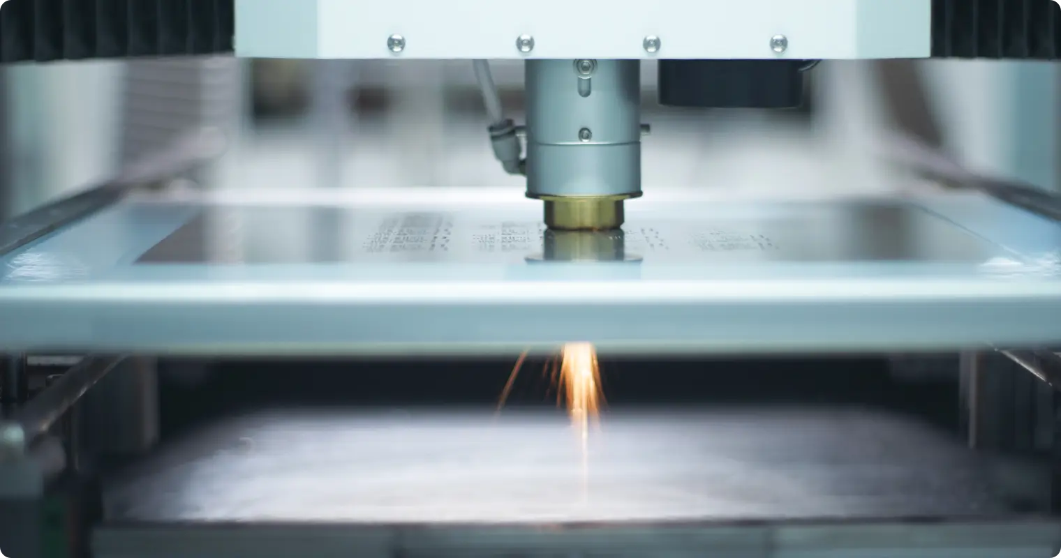
QFN (Quad Flat No-leads) components are widely used in modern electronic designs due to their excellent thermal and electrical performance. However, their hidden pins and large-area thermal pad design also bring two major headaches in SMT soldering: bridging and empty soldering. This article will cut directly to the main points and share the core process know-how to avoid these defects.
1.Avoiding Bridges: Controlling Solder Paste Volume and Spacing
Bridging refers to unwanted solder shorts connecting adjacent pins, which is particularly common in fine-pitch QFNs.
1.1Stencil Design
The essence of bridging is excessive or collapsing solder paste. For QFNs with a pin pitch ≤ 0.4mm, the stencil aperture must be designed with a reduction in size. It is recommended to reduce the aperture width to 80%-90% of the pad width, maintain the original length or slightly indent it, and avoid 1:1 aperture design. Furthermore, the recommended stencil thickness is 0.1mm-0.12mm; if too thick, it will lead to excessive solder paste deposition, increasing the risk of bridging.
1.2 Ensure the Integrity of the Solder Mask Bridge
In PCB design, the solder mask bridge between pin pads is crucial. It must be ensured that the solder mask bridge is complete and wide enough to prevent molten solder from flowing across and causing shorts. The spacing between pin pads and the central thermal pad should also be greater than 0.15mm.
1.3 Placement Accuracy and Pressure
During the placement process, it is necessary to ensure that the device is centered with respect to the pad, and the deviation should be less than 15%. Excessive placement pressure can squeeze and collapse the solder paste, which is also a common cause of bridging.
2.Overcoming Empty Soldering (Including Voids): Creating Exhaust Channels for Large Pads
The large-area soldering of the QFN's central thermal pad is a high-risk area for empty soldering and voids. Voids can affect heat dissipation and even lead to reliability failures.
2.1 Stencil Aperture: Grid Instead of Entire Area
It is strictly prohibited to make large-scale, entire-area aperture for the central thermal pad. A grid pattern (e.g., tic-tac-toe style) or an array of circular apertures must be used. This divides the large soldering area into smaller segments, ensuring adequate total solder paste while creating channels for gases (from flux evaporation) to escape during soldering, significantly reducing the voiding rate. The total aperture area is typically recommended to cover 50%-80% of the thermal pad area.
2.2 Managing Thermal Vias: "Plug" vs. "Wick"
If thermal vias on the PCB are left open, they will wick away molten solder during reflow, leading to empty soldering. Thermal vias must be plugged using a process like filling with solder mask or resin to prevent solder loss.
2.3 Temperature Profile: Allow Enough Activation Time
The reflow profile was adjusted to appropriately extending the time in the soak zone (150-200°C) to about 60-90 seconds. This allows the flux to fully activate and volatilize, reducing the chance of violent outgassing and void formation during the reflow zone. Some studies suggest that appropriately extending the reflow time (e.g., 80 seconds) also helps bubbles escape, reducing voids.
2.4 Solder Paste Selection
For products with extremely strict requirements for void rate, it is advisable to consider using highly reliable solder paste, or even trying pre-formed solder tabs. It doesn’t contain flux, fundamentally eliminating voids caused by flux evaporation.
In summary, solving QFN soldering problems hinges critically on stencil design. By lessening stencil aperture to prevent bridges, using a grid aperture for the thermal pad combined with proper via management to prevent empty soldering, and pairing these with an accurate reflow profile, QFN soldering yield can be effectively improved.
With 16 years of expertise in PCBA design, manufacturing, and service, KingshengPCBA is ready to help turn your ideas into reality. Feel free to contact us anytime to discuss your requirements and get a professional quotation.

Please send Email to kspcba@c-alley.com or call us through +86 13828766801 Or submit your inquiry by online form. Please fill out below form and attach your manufacturing files( PCB Gerber files and BOM List) if need quotation. We will contact you shortly.
 +86 13828766801
 kspcba@c-alley.com
 https://www.kingshengpcba.com/
 2/F, Building 6, Tangtou 3rd Industrial Zone, Tangtou Community, Shiyan Town, Baoan District, Shenzhen, China, 518108
We would also like to thank our customers for their trust and support. The company's outstanding achievements are mainly due to the loyalty of our customers, which also encourages and spurs our company to forge ahead.


