* On your first PCB Assembly order!
* Up to $300 discount
 C - A L L E Y
 Home | Events | PCB | About Us | News | Contact Us
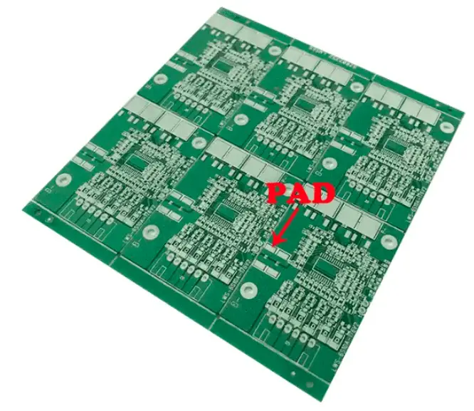
As an operations manager at a PCBA manufacturing plant, we’ve seen firsthand how small design oversights can cause major production headaches. Among all design elements, PCB pad design is one of the most critical yet frequently underestimated factors. A well-designed pad ensures smooth soldering, reliable component connections, and long-term board performance. Poor pad design, however, can lead to solder bridges, tombstoning, insufficient solder joints, and costly rework.
In this post, we’ll break down the key industry standards for PCB pad design and explain how each standard directly impacts manufacturing efficiency and product quality.
IPC-A-610: Acceptability of Electronic Assemblies
IPC-A-610 is the global benchmark for evaluating the acceptability of soldered electronic assemblies, and it includes clear guidelines for pad design. While it doesn’t specify exact pad dimensions, it defines the acceptable outcomes of pad-related manufacturing processes.
Key Requirements:
Manufacturing Impact:
IPC-7351: Generic Requirements for Surface Mount Design and Land Pattern Standard
IPC-7351 is the most comprehensive standard for surface mount device (SMD) pad design. It provides detailed land pattern dimensions for thousands of component types, including resistors, capacitors, QFPs, and BGAs.
Key Requirements:
Manufacturing Impact:
IPC-2221: Generic Standard on Printed Board Design
IPC-2221 is a foundational standard that covers general PCB design principles, including pad design for both through-hole and surface mount components. It provides formulas and guidelines for calculating pad sizes based on component specifications and manufacturing capabilities.
Key Requirements:
Manufacturing Impact:
How Pad Design Standards Impact Our Manufacturing Process
At our PCBA factory, we’ve implemented strict adherence to IPC standards for pad design, and the results speak for themselves:
Conclusion
PCB pad design is far more than just drawing squares on a layout. It’s a critical engineering decision that directly impacts manufacturing efficiency, product quality, and long-term reliability. By following industry standards like IPC-A-610, IPC-7351, and IPC-2221, and incorporating DFM principles, design engineers can create boards that are not only functional but also manufacturable at scale.
As someone who’s spent years on the factory floor, we can’t stress enough how important it is for design teams to collaborate closely with manufacturing partners early in the design process. A little extra attention to pad design can save weeks of rework, reduce costs, and ensure your product performs as intended for years to come.
With 16 years of expertise in PCBA design, manufacturing, and service, KingshengPCBA is ready to help turn your ideas into reality. Feel free to contact us anytime to discuss your requirements and get a professional quotation.

Please send Email to kspcba@c-alley.com or call us through +86 13828766801 Or submit your inquiry by online form. Please fill out below form and attach your manufacturing files( PCB Gerber files and BOM List) if need quotation. We will contact you shortly.
 +86 13828766801
 kspcba@c-alley.com
 https://www.kingshengpcba.com/
 2/F, Building 6, Tangtou 3rd Industrial Zone, Tangtou Community, Shiyan Town, Baoan District, Shenzhen, China, 518108
We would also like to thank our customers for their trust and support. The company's outstanding achievements are mainly due to the loyalty of our customers, which also encourages and spurs our company to forge ahead.


