* On your first PCB Assembly order!
* Up to $300 discount
 C - A L L E Y
 Home | Events | PCB | About Us | News | Contact Us
In PCBA manufacturing, the solder joint is the critical link between the component and the function of the product. As an Operations Manager, I know that a perfect solder joint is not an accident—it is the result of controlled processes. When defects arise, they signal a deviation in the "Input-Process-Output" chain.
Here is a breakdown of 12 common soldering defects, their root causes, and our operational solutions to ensure first-pass yield.
1. Solder Bridges
Cause: Excess solder paste, misaligned stencil, or insufficient wipe frequency.
Solution: Optimize stencil aperture reduction (typically 10%) and ensure proper stencil cleaning. Verify placement accuracy.
2. Cold Solder Joints
Cause: Insufficient heat transfer during reflow or dirty PCB pads preventing wetting.
Solution: Adjust the reflow profile to ensure the solder reaches the correct peak temperature. Check flux activity and pad cleanliness.
3. Solder Balls
Cause: Solder paste spattering due to rapid heating or moisture absorption in the paste.
Solution: Adjust the ramp-up rate in the reflow oven (typically <3°C/sec). Ensure solder paste is stored and thawed correctly.
4. Tombstoning
Cause: Unequal torque on component ends due to asymmetric pad design or uneven paste deposition.
Solution: Redesign footprints for symmetry. Check squeegee pressure and stencil condition to ensure uniform paste volume.
5. Insufficient Solder
Cause: Clogged stencil apertures or low squeegee pressure during printing.
Solution: Implement regular underside stencil wiping. Verify squeegee pressure and speed; inspect for stencil wear.
6. Excess Solder
Cause: Stencil aperture too large or "squeeze-out" caused by poor gasketing between stencil and PCB.
Solution: Reduce stencil aperture size. Check the stencil fixture to ensure a tight seal on the PCB surface.
7. Voiding (Bubbles)
Cause: Entrapped flux or gas, common on large thermal pads (QFNs/BGAs).
Solution: Optimize the reflow profile to allow gases to escape before the solder solidifies. Use "micro-vias in pad" designs or vacuum reflow technology.
8. Open Joints (Skips)
Cause: Component coplanarity issues (leads bent up) or insufficient paste height.
Solution: Inspect component leads before placement. Increase paste height or adjust placement force to ensure contact.
9. Cracked Solder Joints
Cause: Mechanical stress during depaneling or thermal shock during cooling.
Solution: Review handling procedures to minimize mechanical shock. Control the cooling zone rate to prevent thermal stress.
10. Lifted Pads
Cause: Overheating during rework or excessive mechanical force.
Solution: Strictly control soldering iron temperature and dwell time. Use proper tools for lifting operations.
11. Pinholes
Cause: Moisture trapped in the PCB substrate or plating imperfections.
Solution: Bake PCBs prior to assembly to remove moisture (per IPC standards). Audit raw board plating quality.
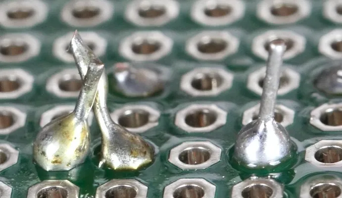
12. Solder Wicking
Cause: The component lead heats up faster than the PCB pad, drawing solder away.
Solution: Adjust the reflow profile to ensure the pad reaches reflow temperature simultaneously with the lead. Use nitrogen atmosphere to improve wetting.
Conclusion
Soldering defects are rarely random; they are data points indicating where our process needs attention. By understanding these 12 common issues, we move from reactive "firefighting" to proactive quality assurance. At our facility, we combine SPI (Solder Paste Inspection) and AOI (Automated Optical Inspection) to catch these issues early, ensuring that every board we ship is built to last.
With 16 years of expertise in PCBA design, manufacturing, and service, KingshengPCBA is ready to help turn your ideas into reality. Feel free to contact us anytime to discuss your requirements and get a professional quotation.

Please send Email to kspcba@c-alley.com or call us through +86 13828766801 Or submit your inquiry by online form. Please fill out below form and attach your manufacturing files( PCB Gerber files and BOM List) if need quotation. We will contact you shortly.
 +86 13828766801
 kspcba@c-alley.com
 https://www.kingshengpcba.com/
 2/F, Building 6, Tangtou 3rd Industrial Zone, Tangtou Community, Shiyan Town, Baoan District, Shenzhen, China, 518108
We would also like to thank our customers for their trust and support. The company's outstanding achievements are mainly due to the loyalty of our customers, which also encourages and spurs our company to forge ahead.


