* On your first PCB Assembly order!
* Up to $300 discount
 C - A L L E Y
 Home | Events | PCB | About Us | News | Contact Us
In the electronics manufacturing industry, solder short circuits are a common cause of product failures. As a tiny structure on a printed circuit board (PCB), the precision control of the solder mask bridge directly determines the quality of the soldering process. Today, we'll delve into how to effectively avoid solder short circuits through high-precision solder mask bridge control.
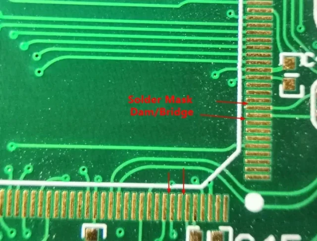
What is a Solder Mask Bridge?
A solder mask bridge is a tiny strip of solder mask material on the solder mask layer of a PCB, positioned between two adjacent pads. Its function is to physically isolate the pads, preventing molten solder from flowing and causing short circuits during soldering. With the increasing miniaturization of electronic components, the width of solder mask bridges has shrunk from 100μm to 50μm or even smaller, placing extremely high demands on precision control.
Three Key Precision Control Points to Avoid Solder Short Circuits
1. Preventative Planning in the Design Phase
Optimize Solder Mask Bridge Size: According to the IPC-2221 standard, the minimum width of a solder mask bridge should not be less than 0.1mm (100μm). For high-density boards, the spacing can be appropriately reduced to 75-80μm, but manufacturing capabilities need to be assessed.
Optimize pad spacing: When the pad center-to-center distance is less than 0.25mm, it is recommended to use solder mask defined pads (SMD) instead of copper defined pads (NSMD) to enhance the stability of the solder mask bridges.
Consider thermal effects: The design of solder mask bridges should take into account the thermal expansion during reflow soldering. The width of the solder mask bridges in key areas should be appropriately increased by 10-15% to prevent cracking of the solder mask layer due to thermal stress.
2. Key technology control in the manufacturing process
Exposure accuracy management: Using LDI (Laser Direct Imaging) technology instead of traditional exposure can improve the alignment accuracy to within ±15μm, ensuring precise solder mask bridge positioning.
Screen printing parameter optimization:
*Select a 150-180T screen, paired with a 25-30μm thick latex layer.
*Control the solder resist ink viscosity to 90-110 Pa·s (25℃).
*Maintain a squeegee angle of 60°±5° and a speed of 50-80mm/s.
Precise curing process: Segmented curing reduces internal stress in the solder resist layer. A stepped temperature increase is recommended: 80℃ (pre-baking for 20 minutes) → 100℃ (15 minutes) → final curing (150℃, 45-60 minutes).
3. Quality inspection and feedback adjustment
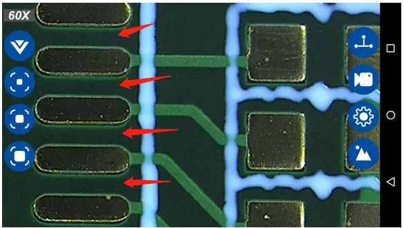
AOI: An AOI system with a resolution of 10 μm is adopted to inspect the integrity, width consistency and edge clarity of the solder mask bridges.
Key monitoring areas: Special attention should be paid to the quality of the solder bridges between the pins of QFP and BGA packages, as well as between the pads of components with dimensions below 0402. Establish a process feedback loop: Classify and statistically analyze detected solder mask bridge defects by location and type, analyze trends weekly, and adjust upstream process parameters promptly. Practical Tips: Quickly Troubleshoot Solder Mask Bridge Issues
When solder short circuits occur, troubleshoot solder mask bridge issues using the following procedure:
1.Check the design: Confirm whether the solder mask bridge design conforms to DFM rules, especially for adjacent pads with a spacing of less than 0.3mm;
2.Check alignment: Check for solder mask bridge misalignment, using a microscope to observe the distance between the solder mask layer and the pad edge;
3.Measure thickness: Use a film thickness gauge to check whether the solder mask layer thickness is uniform, with a target value of 15-25μm;
4.Check adhesion: Perform a tape test to confirm that the solder mask layer is firmly bonded to the substrate, without blistering or peeling;
Conclusion
Although the solder bridge is small, it is the key defense line for the welding quality. Through the full-process precision management of "design prevention - process control - inspection feedback", we can reduce the solder short circuit caused by the solder bridge problem by more than 90%. In today's era of increasingly sophisticated electronic devices, attaching importance to these tiny details is precisely an important way to enhance product reliability.
With 16 years of expertise in PCBA design, manufacturing, and service, KingshengPCBA is ready to help turn your ideas into reality. Feel free to contact us anytime to discuss your requirements and get a professional quotation.

Please send Email to kspcba@c-alley.com or call us through +86 13828766801 Or submit your inquiry by online form. Please fill out below form and attach your manufacturing files( PCB Gerber files and BOM List) if need quotation. We will contact you shortly.
 +86 13828766801
 kspcba@c-alley.com
 https://www.kingshengpcba.com/
 2/F, Building 6, Tangtou 3rd Industrial Zone, Tangtou Community, Shiyan Town, Baoan District, Shenzhen, China, 518108
We would also like to thank our customers for their trust and support. The company's outstanding achievements are mainly due to the loyalty of our customers, which also encourages and spurs our company to forge ahead.


