* On your first PCB Assembly order!
* Up to $300 discount
 C - A L L E Y
 Home | Events | PCB | About Us | News | Contact Us
PCB (Printed Circuit Board) technology, which has evolved since the early 20th century, has become an indispensable foundation for modern electronic devices. It is widely used in numerous fields such as computers, communications, and consumer electronics. With technological advancements, PCBs have progressed from single-layer designs to double-sided, multi-layer, and even flexible designs, continuously striving for higher precision, density, and reliability. This developmental trend ensures that PCBs continue to play a crucial role in the miniaturization and high-performance evolution of electronic devices.
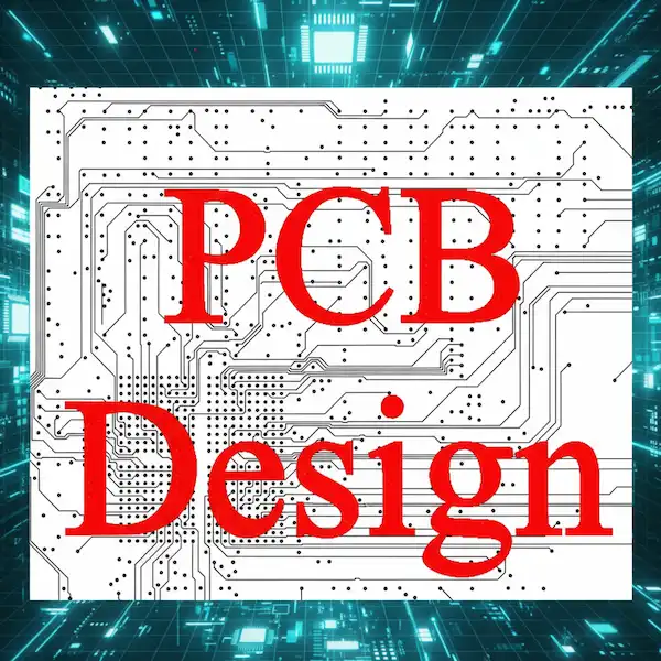
The process of designing a PCB is divided into seven main steps:
1.Preparatory Work: The first step in designing a PCB is preparing the component library and schematic diagram.
The component library contains models of all electronic components to be used, including the PCB component footprint library and the schematic SCH component library. The footprint library must be accurately created based on the actual dimensions of the components to ensure the correct assembly of the PCB later. The schematic library, on the other hand, is used to depict the logical connections of the circuit, paying attention to pin attribute definitions and their correspondence with the footprint library.
2.PCB Structure Design: At this stage, the designer determines the dimensions and mechanical positioning of the circuit board, outlines the PCB frame, and places necessary connectors, buttons, switches, etc. Additionally, routing and non-routing areas are defined to ensure the rationality of the design.
3.PCB Layout Design: Layout design involves arranging the components from the schematic diagram reasonably on the PCB board. The netlist is imported, and all components are placed. This step significantly impacts circuit performance and requires consideration of factors such as signal flow, thermal management, and interference suppression.
4.PCB Routing Design: Routing is a core part of PCB design and includes three aspects: ensuring connectivity, optimizing electrical performance, and improving aesthetics. First, all electrical connections between components must be correctly established. Next, routing is adjusted to optimize electrical performance. Finally, the routing is organized neatly to facilitate debugging and maintenance in later stages.
5.Routing Optimization and Silkscreen Placement: After routing is completed, the design needs to be optimized, which may involve multiple adjustments to balance various design requirements. Meanwhile, silkscreen markings are added, with clear distinctions between the top and bottom layers. The bottom-layer silkscreen requires mirroring.
6.Netlist DRC and Structural Check: This is a critical step for quality control. Design Rule Checking (DRC) is performed to ensure that the routing complies with design specifications and avoids issues such as short circuits or excessive density. Structural elements are also checked to ensure they meet physical installation requirements.
7.Final Check and Output: After a comprehensive review to confirm accuracy, Gerber files are exported for PCB manufacturing. Additionally, design documentation, such as design reports and component lists, is compiled to support subsequent production and maintenance.
The above seven steps form the basic workflow of PCB design. Each step is crucial and requires designers to possess profound circuit knowledge and practical experience. Through meticulous design, PCBs that meet functional requirements, exhibit excellent electrical performance, and are easy to manufacture can be produced.
Professional PCB Design & PCB Manufacturing
KingshengPCBA is a factory located in Shenzhen, China, with 16 years of experience in OEM manufacturing. We provide high-quality products and services to customers across various industries.
Our products include PCB bare boards, PCB assembly, box building, electronic components, metal and enclosure parts, cables, wires, and housings.
Our services cover alternative material solutions, BOM optimization, PCB design and layout, design optimization, and DFM/DFT.
If you have new projects requiring a quotation, please feel free to contact us at www.kingshengpcba.com.
With 16 years of expertise in PCBA design, manufacturing, and service, KingshengPCBA is ready to help turn your ideas into reality. Feel free to contact us anytime to discuss your requirements and get a professional quotation.

Please send Email to kspcba@c-alley.com or call us through +86 13828766801 Or submit your inquiry by online form. Please fill out below form and attach your manufacturing files( PCB Gerber files and BOM List) if need quotation. We will contact you shortly.
 +86 13828766801
 kspcba@c-alley.com
 https://www.kingshengpcba.com/
 2/F, Building 6, Tangtou 3rd Industrial Zone, Tangtou Community, Shiyan Town, Baoan District, Shenzhen, China, 518108
We would also like to thank our customers for their trust and support. The company's outstanding achievements are mainly due to the loyalty of our customers, which also encourages and spurs our company to forge ahead.


