* On your first PCB Assembly order!
* Up to $300 discount
 C - A L L E Y
 Home | Events | PCB | About Us | News | Contact Us
Keywords: electronic potting compound, potting compound for PCBA, epoxy vs silicone vs polyurethane potting, potting compound vs gap filler pad.
A Technical Overview for PCBA and Electronics Manufacturing
Meta Description (SEO suggestion): Learn what electronic potting compounds are, how epoxy, silicone, and polyurethane potting materials differ, and how to choose the right potting compound for PCBA protection and thermal management.
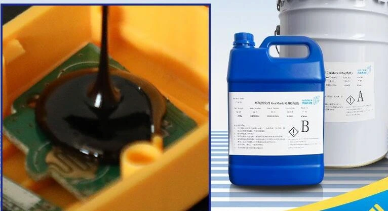
Potting is a process in which a liquid polymer compound is poured—manually or mechanically—into an enclosure containing electronic components and circuitry. The compound then cures at room temperature or under heat, forming a thermoset polymer insulation system with excellent protective and electrical properties.
In electronics manufacturing, potting compounds are primarily used to replace air voids, enhance environmental protection, and ensure reliable thermal transfer. The three most common types of electronic potting compounds are:
1. Potting Compounds vs. Gap-Filler Pads
The primary function of a potting compound is to eliminate air gaps while providing mechanical protection and thermal management. However, potting is not the only available solution. Gap-filler pads are another widely used thermal interface material in electronics.
Both potting compounds and gap-filler pads offer effective thermal management, but their mechanical behavior, form factor, and process compatibility differ significantly. Although gap-filler pads have a longer history in electronics, recent advancements in potting materials have allowed them to outperform pads in certain applications.
2. Comparative Analysis: Potting Compounds vs. Gap-Filler Pads
2.1 Conformability and Filling Capability
Both materials exhibit some degree of conformability. However, because gap-filler pads are solid materials, their maximum adaptability is inherently limited. Potting compounds, being liquid prior to curing, can fully encapsulate components and penetrate complex internal gaps, making them more suitable for densely populated or irregular assemblies.
2.2 Precision and Shape Control
Gap-filler pads can be die-cut into precise shapes that match customer-specific parts, which is advantageous in simple and planar assemblies. In complex layouts—where components vary in height or wiring is dense—pads can only provide surface contact, leaving internal voids unfilled.
Potting compounds, by contrast, are applied via pouring or dispensing. During curing, polymer chains form a tightly bonded network, creating strong adhesion that resists separation by external forces. The final shape of a potting compound is determined by the enclosure itself, enabling excellent shape conformity and application flexibility.
2.3 Cost and Manufacturing Efficiency
From an application standpoint, potting compounds offer broader versatility and a clear advantage in automation. Gap-filler pads typically require custom cutting and manual placement, with strict orientation requirements (top/bottom, left/right). This increases labor cost and the risk of human error.
As labor costs continue to rise, the automation compatibility of potting compounds becomes increasingly valuable. While potting materials were historically more expensive than pads, continuous raw material optimization has significantly reduced their cost. Today, on a volume-equivalent basis, potting compounds are often more cost-effective than comparable gap-filler pads.
3. Why Potting Compounds Are Gaining Market Share
For many years, gap-filler pads were the default choice for electronics engineers. However, potting compounds now offer:
Superior environmental protection
Improved manufacturability and assembly efficiency
Competitive or lower cost in high-volume applications
As a result, potting compounds are increasingly replacing gap-filler pads in demanding electronic systems.
4. Main Types of Electronic Potting Compounds
4.1 Epoxy Potting Compounds
Epoxy potting compounds are primarily composed of bisphenol-A epoxy resin, curing agents (amines or anhydrides), reinforcing additives, and fillers.
Advantages: - Low viscosity and excellent penetration into fine gaps - Long pot life, suitable for automated mass production - Minimal filler sedimentation during curing - Low exothermic peak and low curing shrinkage - Flame retardant, weather resistant, and thermally conductive - Strong adhesion to metals and many substrates - Low water absorption
Limitations: - Poor resistance to thermal cycling - High hardness and brittleness after curing - Generally considered a permanent (“lifetime”) encapsulation material
4.2 Silicone Potting Compounds
Silicone potting compounds consist mainly of silicone resins, crosslinkers, catalysts, and optional thermally conductive fillers. Both single-component and two-component systems are available.
Advantages: - No by-products and no shrinkage during curing - Excellent electrical insulation - Wide operating temperature range (−50°C to 200°C) - Semi-gel state after curing, offering superior thermal shock resistance - Long working time after mixing; curing speed can be heat-controlled - Self-healing behavior after mechanical cracking - Excellent reworkability—components can be removed and replaced Limitations: - Relatively weak adhesion compared with epoxy and PU systems
4.3 Polyurethane (PU) Potting Compounds
Polyurethane potting compounds are typically synthesized from polyester or polyether polyols reacted with diisocyanates, using diols or diamines as chain extenders.
Advantages: - Low hardness with moderate strength and good elasticity - Excellent vibration damping and shock absorption - Good water resistance, mold resistance, and electrical insulation - Flame retardant and non-corrosive to electronic components - Strong adhesion to metals (steel, aluminum, copper, tin) and many plastics
Limitations: - Limited high-temperature resistance - Prone to bubbling - Poor UV resistance; discoloration over time - Moisture-sensitive before curing; requires dry processing conditions
5. Application Methods for Potting Compounds
After curing, potting compounds significantly enhance the structural integrity of electronic assemblies, allowing them to withstand shock, vibration, moisture, dust, and chemical exposure.
5.1 Single-Component Potting Compounds
Recommended procedure: 1. Conduct small-scale adhesion tests before full application. 2. Thoroughly clean bonding surfaces to remove contaminants. 3. During machine dispensing, prevent moisture ingress if dispensing is paused. 4. Curing speed depends on ambient temperature; higher temperature and humidity can accelerate curing.
5.2 Two-Component (A/B) Potting Compounds
Recommended procedure: 1. Ensure the product to be potted is clean and dry. 2. Mix components strictly by weight ratio, not volume, and stir thoroughly. 3. Dispense immediately after mixing and use within the specified pot life. 4. Allow the compound to penetrate gaps; perform secondary potting if required. 5. Maintain a clean environment during curing to avoid surface contamination. 6. Seal unused material immediately after application for future use.
6. Application Fields and Market Outlook
Thanks to their excellent elasticity, toughness, and protective performance, potting compounds are widely used not only in electronics, but also in:
New energy systems
According to market data, the global potting compound market reached USD 3.21 billion in 2020 and is projected to grow to USD 3.70 billion by 2026, with a compound annual growth rate (CAGR) of approximately 3.6%.
7. How to Choose the Right Potting Compound for Your PCBA
When selecting a potting compound for electronic assemblies, engineers should evaluate both material properties and process requirements. Key decision factors include:
Operating temperature range: Silicone compounds are preferred for extreme high/low temperatures.
Vibration and mechanical stress: Polyurethane offers superior elasticity and shock absorption.
Rework and maintenance needs: Silicone allows easier component removal and repair.
Environmental exposure: Epoxy provides excellent moisture and chemical resistance.
Production volume and automation: Epoxy and silicone systems are well suited for automated dispensing lines.
There is no universal solution. The optimal potting compound depends on the balance between reliability, manufacturability, and cost.
8. Frequently Asked Questions (FAQ)
What is an electronic potting compound?
An electronic potting compound is a liquid polymer material used to encapsulate electronic components. After curing, it provides mechanical protection, electrical insulation, and environmental sealing. What is the difference between potting compounds and gap-filler pads?
Potting compounds are liquid before curing and can fully fill complex internal gaps, while gap-filler pads are solid materials mainly used for surface-level thermal interface applications.
Which potting compound is best for PCBA?
There is no single best option. Epoxy, silicone, and polyurethane potting compounds each serve different PCBA requirements depending on temperature, vibration, reworkability, and cost.
Can potting compounds improve thermal management?
Yes. When formulated with thermally conductive fillers, potting compounds can effectively transfer heat while eliminating air voids that reduce thermal efficiency.
Are potting compounds suitable for mass production?
Yes. Most modern potting compounds are designed for automated dispensing and curing, making them suitable for high-volume PCBA manufacturing.
Final Takeaway
Potting compounds have evolved into a critical material technology for high-reliability PCBA and electronic systems. Compared with gap-filler pads, they offer superior conformability, automation compatibility, and long-term environmental protection.
For independent websites targeting overseas PCBA customers, publishing in-depth, engineering-driven content like this not only improves search visibility but also builds long-term technical credibility with OEM and EMS partners.
With 16 years of expertise in PCBA design, manufacturing, and service, KingshengPCBA is ready to help turn your ideas into reality. Feel free to contact us anytime to discuss your requirements and get a professional quotation.

Please send Email to kspcba@c-alley.com or call us through +86 13828766801 Or submit your inquiry by online form. Please fill out below form and attach your manufacturing files( PCB Gerber files and BOM List) if need quotation. We will contact you shortly.
 +86 13828766801
 kspcba@c-alley.com
 https://www.kingshengpcba.com/
 2/F, Building 6, Tangtou 3rd Industrial Zone, Tangtou Community, Shiyan Town, Baoan District, Shenzhen, China, 518108
We would also like to thank our customers for their trust and support. The company's outstanding achievements are mainly due to the loyalty of our customers, which also encourages and spurs our company to forge ahead.


