* On your first PCB Assembly order!
* Up to $300 discount
 C - A L L E Y
 Home | Events | PCB | About Us | News | Contact Us
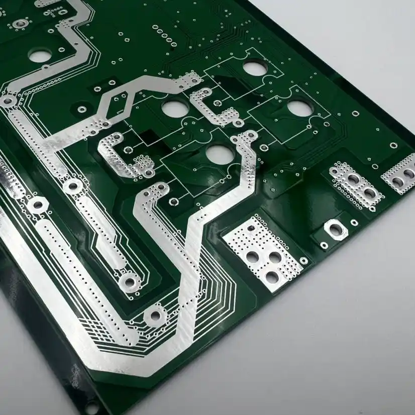
I. Basic Logic of Multilayer PCB Copying
The essence of copying a multilayer PCB lies in deconstructing its complex internal structure into combinations of multiple double-sided boards. For example, a 4-layer board can be regarded as the superposition of two double-sided boards, a 6-layer board as three double-sided boards, and so on. The primary challenge in copying multilayer boards stems from the invisibility of internal traces, which necessitates delamination techniques to expose the internal circuitry.
II. Choice of Delamination Technology: Advantages of Sandpaper Grinding
Delamination is the core step in visualizing the internal layers of a multilayer PCB. Common methods include chemical corrosion and blade stripping, but these often risk damaging internal traces or losing data due to over-processing. Practical experience has shown that sandpaper grinding is currently the most accurate, economical, and widely adopted delamination solution.
III. Key Operational Points of Sandpaper Grinding
Tool Preparation: Ordinary sandpaper available at hardware stores is sufficient.
Operation Process: Typically, lay the PCB flat, hold the sandpaper, and grind evenly across the PCB surface.
For smaller boards, the sandpaper can be laid flat with the PCB placed on top (or vice versa).
Apply even pressure and grind repeatedly in the same direction. For very small boards, use fingers to press and move the PCB against the sandpaper.
The key is to maintain a flat surface and ensure uniform grinding.
Grinding Effect: The silkscreen and solder mask layers usually wear off quickly, while copper traces and planes require additional grinding.
Time Reference: Bluetooth boards take a few minutes, while memory modules may require over ten minutes.
IV. Specific Steps for Copying a 4-Layer Board
Surface Layer Scanning: Scan the top and bottom layer images of the 4-layer board.
Surface Layer Copying: Complete the replication of the top and bottom layer circuits.
Grinding Delamination: Use sandpaper to grind away the top and bottom layers, exposing the two inner layers.
Inner Layer Scanning: Scan the images of the exposed inner layers.
Inner Layer Copying: Add the inner layers in the copying software and replicate their circuitry.
Final Inspection: Cross-check each layer’s traces to ensure copying accuracy.
Note: PCBs with more layers can be processed similarly, with workload increasing proportionally to the number of layers.
V. Key Techniques and Precautions for Multilayer PCB Copying
Cost and Risk: The manufacturing cost of multilayer boards is significantly higher than that of double-sided boards (often several times higher). Additionally, internal trace errors are difficult to repair with jumpers.
Prioritize Accuracy: Strictly verify the circuitry of each layer during copying to avoid minor errors causing complete board failure.
Experience Accumulation: Mastering the pressure and uniformity of sandpaper grinding is essential for ensuring delamination quality.
By following the above methods, the technical challenges of copying multilayer PCBs can be effectively addressed. However, attention to operational details is crucial to mitigate risks and ensure the reliability of the final outcome.
Professional Reverse Engineering & PCB Manufacturing
KingshengPCBA specializes in reverse engineering for all PCB types — including single-sided, double-sided, and multilayer boards. We provide full production support according to your required quantities and supply all necessary components. Upon completion, we deliver all project files and ensure expedited processing.
PCB samples are personally delivered by our project manager for your verification.
For detailed information, visit us at: www.kingshengpcba.com
With 16 years of expertise in PCBA design, manufacturing, and service, KingshengPCBA is ready to help turn your ideas into reality. Feel free to contact us anytime to discuss your requirements and get a professional quotation.

Please send Email to kspcba@c-alley.com or call us through +86 13828766801 Or submit your inquiry by online form. Please fill out below form and attach your manufacturing files( PCB Gerber files and BOM List) if need quotation. We will contact you shortly.
 +86 13828766801
 kspcba@c-alley.com
 https://www.kingshengpcba.com/
 2/F, Building 6, Tangtou 3rd Industrial Zone, Tangtou Community, Shiyan Town, Baoan District, Shenzhen, China, 518108
We would also like to thank our customers for their trust and support. The company's outstanding achievements are mainly due to the loyalty of our customers, which also encourages and spurs our company to forge ahead.


