* On your first PCB Assembly order!
* Up to $300 discount
 C - A L L E Y
 Home | Events | PCB | About Us | News | Contact Us
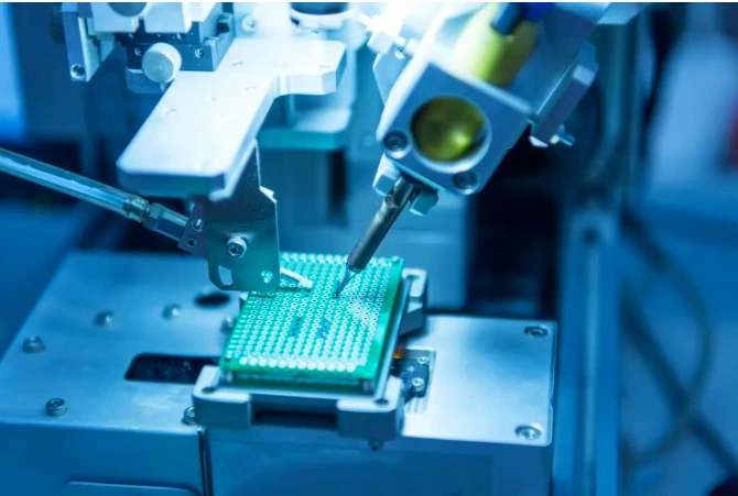
Wave soldering is essential for assembling through-hole components and mixed-assembly PCBs. The process directly affects soldering quality and product reliability. At KINGSHENG PCBA, we have set up clear technical standards for wave soldering, covering equipment settings, materials management, process monitoring, and quality checks. These standards ensure we consistently meet the soldering needs of various products.
1.Equipment and Parameter Control
The condition of wave soldering equipment is crucial for process stability. At KINGSHENG PCBA, we control the preheating, soldering, and cooling zones. Preheating is set between 90-130°C, with a ramp-up of 1.5-3°C per second. The soldering zone stays at 245-260°C, with a fluctuation of ±3°C. The cooling zone ensures solder joints drop below 100°C within 60 seconds.
The wave height is adjusted according to PCB thickness and layout, typically between 1/2 to 2/3 of the PCB thickness. The conveyor belt tilts at 4-7 degrees, with speed adjustable from 0.8 to 1.8 meters per minute. These settings help reduce defects like bridging and solder voids.
2.Process Materials Management
The choice of solder alloy affects both quality and cost. At KINGSHENG PCBA, we use lead-free solder alloys like SAC305 or SAC307, following RoHS guidelines. The solder bath’s composition is analyzed daily, ensuring copper content is under 0.3% and iron content under 0.02%.
Flux selection depends on the product’s application. For commercial products, we use ROL0 no-clean flux; for industrial products, we use ROL1 active flux; and for high-end applications like automotive electronics, we choose low-residue flux with specialized formulas. Flux is applied through a controlled spraying system, covering 80% of the pad area without dripping.
3. Process Monitoring and Technical Standards
Real-time monitoring is crucial for consistent soldering. Our wave soldering machines are equipped with a 12-point temperature monitoring system. Thermocouples are placed on the top and bottom layers, as well as on critical component pins, with real-time data uploaded to the MES system.
The dross removal system uses nitrogen protection and mechanical skimming to keep solder dross below 1.5% of the total solder volume. For different PCB types, the fixtures are designed with ±0.2mm positioning accuracy, avoiding test points and sensitive components, and are temperature-resistant up to 300°C for continuous use.
4. Quality Verification and Process Optimization
Soldering quality is verified using multiple standards. For macro inspection, the solder joint fill should be over 75%, with lead exposure between 0.5-2.0mm. Microscopic analysis includes cross-sectional tests to check the intermetallic compound (IMC) layer, which should be 1-4µm thick.
We use a parameter optimization model and Design of Experiments (DOE) to find the best settings. For special PCBs, like thick copper or metal base boards, we have specific soldering solutions, such as longer preheating times and adjusted wave profiles.
5. Continuous Improvement and Technological Innovation
Wave soldering improvement is an ongoing process. Each month, we analyze soldering defects, identify issues, and take corrective actions. We are also exploring new technologies like inert gas protection soldering and selective wave soldering.
With these strict technical requirements, we have achieved a 99.2% wave soldering pass rate, ensuring reliable processes for high-quality products. As part of our smart manufacturing transformation, we plan to enhance the digital management of wave soldering. By using big data analysis, we aim to predict deviations, implement preventive maintenance, and make adjustments to provide more stable and reliable soldering solutions for our customers.
Conclusion
Wave soldering is a key process in PCBA manufacturing, requiring careful management of equipment, materials, and quality control. At KINGSHENG PCBA, we use advanced techniques and best practices to optimize this process. Through ongoing improvements and innovation, we ensure reliable, high-quality results that meet our customers’ needs, enhancing their product success and competitiveness.
With 16 years of expertise in PCBA design, manufacturing, and service, KingshengPCBA is ready to help turn your ideas into reality. Feel free to contact us anytime to discuss your requirements and get a professional quotation.

Please send Email to kspcba@c-alley.com or call us through +86 13828766801 Or submit your inquiry by online form. Please fill out below form and attach your manufacturing files( PCB Gerber files and BOM List) if need quotation. We will contact you shortly.
 +86 13828766801
 kspcba@c-alley.com
 https://www.kingshengpcba.com/
 2/F, Building 6, Tangtou 3rd Industrial Zone, Tangtou Community, Shiyan Town, Baoan District, Shenzhen, China, 518108
We would also like to thank our customers for their trust and support. The company's outstanding achievements are mainly due to the loyalty of our customers, which also encourages and spurs our company to forge ahead.


