* On your first PCB Assembly order!
* Up to $300 discount
 C - A L L E Y
 Home | Events | PCB | About Us | News | Contact Us
Even the most rigorous production processes in PCB assembly inevitably encounter failures. A valuable circuit board suddenly malfunctioning may conceal various problems from design to materials. Failure analysis (FA) is to locate these issues. Today, we'll discuss common methods and real cases for PCB failure analysis.
I. Four Core Analysis Methods
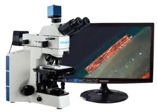
1. Visual Inspection
This is the initial and most direct step. Optical and electron microscopes are used to inspect solder joint cracks, component damage, PCB deformation, etc.
Key Technical Points:
*Using a 3D microscope to measure solder joint height and shape;
*Paying attention to the integrity and collapse degree of BGA component solder balls;
*Checking for solder mask peeling and discoloration;
2. Electrical Testing
Locating the fault area by simulating actual working conditions.
Common Methods:
*Flying Probe Testing: Precisely locates open/short circuits;
*Thermal Imaging: Captures overheated components (hot spots usually indicate overcurrent or short circuits);
*IV Curve Analysis: Compares characteristic curves of good and defective products;
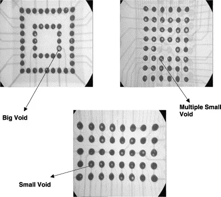
3.Cross-Sectioning
After cutting, polishing, and etching the suspected area, observe the internal structure under a microscope.
Problems that may be detected:
*Internal voids and cracks in solder;
*Excessive or abnormal thickness of IMC (Intermetallic Compound) layer;
*Copper foil separation in PCB inner layers, hole wall cracks;
4.Material and Composition Analysis
When there was suspicion about the material quality, professional equipment is used for in-depth analysis.
Typical Equipment and Applications:
*SEM-EDS: Analyzes foreign matter composition and solder contamination;
*FTIR: Identifies organic contaminants (such as flux residue);
*X-ray fluorescence spectroscopy: Quantitatively analyzes solder alloy ratios;
II. Real Case Analysis
Case 1: Intermittent Failure of BGA
Phenomenon: The communication module performs intermittently during temperature cycling testing.
Analysis Process:
1.Electrical testing revealed an open circuit in a specific data line at high temperature.
2.X-ray showed a tiny crack inside the BGA solder ball.
3.Cross-sectional analysis confirmed the crack was located at the interface between the solder ball and the PCB pad.
4.SEM-EDS revealed abnormal phosphorus enrichment at the interface.
Root Cause: An abnormal ENIG (chemical nickel-gold) process on the PCB pads resulted in excessively high phosphorus content in the nickel layer, forming a brittle interface that cracked under thermal stress.
Solution: Adjust the ENIG flux parameters and strengthen incoming material inspection.
Case 2: Power Module Burnout
Phenomenon: MOSFETs burned out immediately upon power-up in a new batch of products.
Analysis Process:
1.Visual inspection revealed blackened solder joints on the MOSFET leads.
2.Thermal imaging showed abnormally high local temperatures at the moment of power-up.
3.Electrical testing revealed an abnormal gate drive signal.
4.Ultimately, a tiny copper wire short circuit (originating from drilling burrs) was found in the inner layer of the PCB.
Root Cause: Improper drilling parameters during PCB manufacturing produced copper burrs, causing a short circuit between the inner power and signal layers.
Solution: Optimize drilling processes and increase AOI inspection of inner layers.
III. Failure Analysis Process Recommendations
1. First non-destructive then destructive: Try to narrow down the scope using non-destructive methods such as visual inspection and electrical testing as much as possible.
2. Deduce the cause from the phenomenon: Record all information such as environmental conditions and electrical parameters at the time of failure.
3. Team collaboration: FA requires the joint participation of design, process, and materials engineers.
4. Establish a knowledge base: Archive each FA result to form an internal case database.
Failure analysis is not just about solution, but also about preventing future problems. Every in-depth FA paves the way for more reliable products. In the sophisticated and complex world of electronics, this ability to unravel the truth is the core of manufacturing competitiveness.
With 16 years of expertise in PCBA design, manufacturing, and service, KingshengPCBA is ready to help turn your ideas into reality. Feel free to contact us anytime to discuss your requirements and get a professional quotation.

Please send Email to kspcba@c-alley.com or call us through +86 13828766801 Or submit your inquiry by online form. Please fill out below form and attach your manufacturing files( PCB Gerber files and BOM List) if need quotation. We will contact you shortly.
 +86 13828766801
 kspcba@c-alley.com
 https://www.kingshengpcba.com/
 2/F, Building 6, Tangtou 3rd Industrial Zone, Tangtou Community, Shiyan Town, Baoan District, Shenzhen, China, 518108
We would also like to thank our customers for their trust and support. The company's outstanding achievements are mainly due to the loyalty of our customers, which also encourages and spurs our company to forge ahead.


