* On your first PCB Assembly order!
* Up to $300 discount
 C - A L L E Y
 Home | Events | PCB | About Us | News | Contact Us
Within the PCBA manufacturing process, the testing phase constitutes one of the critical steps in ensuring product quality. As the design complexity of electronic products continues to increase, traditional manual inspection methods can no longer meet the demands for rapid, high-precision testing. Automated Optical Inspection (AOI), as an efficient, non-contact inspection technology, is being widely adopted in PCBA testing. This article will provide a detailed examination of the significance of AOI in PCBA manufacturing, its application scenarios, and the advantages it delivers.
1. The fundamental principles of automatic optical inspection (AOI)
1.1 What is Automated Optical Inspection (AOI)?
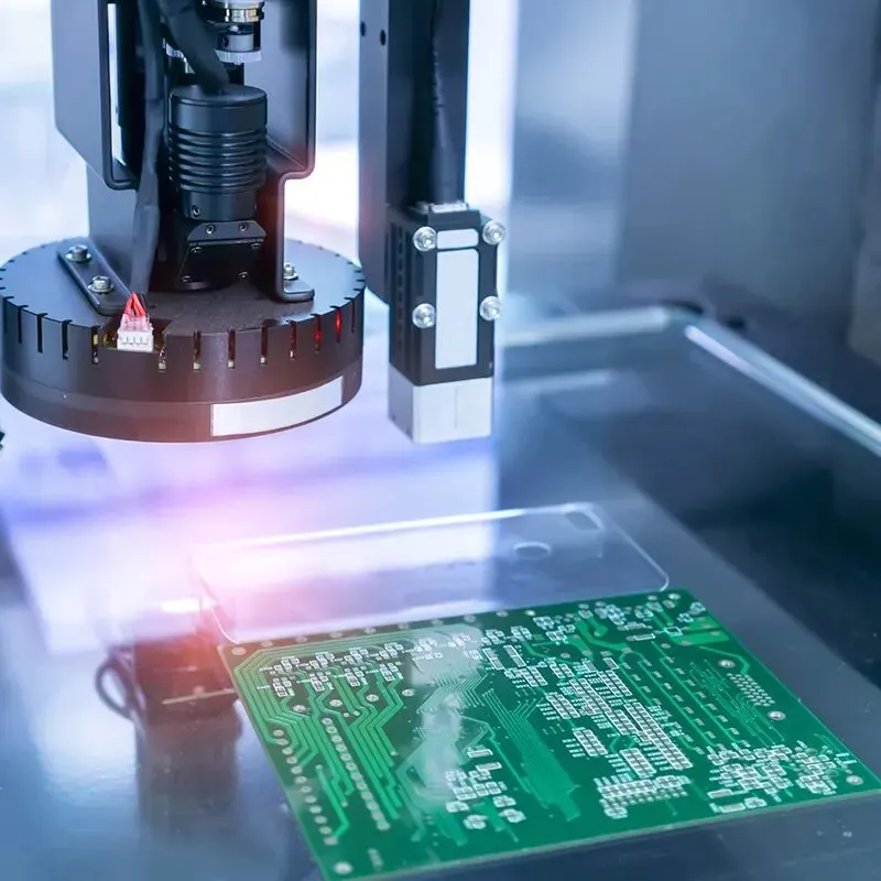
Automated Optical Inspection (AOI) is a technique that employs optical cameras and imaging algorithms to examine the appearance of printed circuit board assemblies (PCBA). AOI is primarily used to identify defects such as soldering faults, component misplacement, short circuits, and open circuits. It relies on high-speed cameras capturing images of the PCBA, which are then analysed by software. These images are compared against standard reference images to detect potential defects.
As a non-contact inspection method, AOI avoids physical damage to circuit boards, making it highly suitable for the demands of modern high-density, high-complexity PCB assembly manufacturing.
1.2 AOI Inspection Methods
AOI inspection primarily comprises two methods: 2D inspection and 3D inspection. 2D AOI analyses the appearance of solder joints, component positioning, and orientation through planar image analysis, making it suitable for visual inspection of simple circuit boards. Conversely, 3D AOI captures multi-angle, three-dimensional images of the circuit board, enabling detection of solder joint height, volume, and other dimensional information. This approach is particularly well-suited for inspecting complex multilayer PCBs and precision solder joints.
2. Application Scenarios of AOI in PCBA Processing
2.1 Solder Joint Inspection
In PCBA manufacturing, solder joint quality directly impacts circuit board performance and reliability. AOI employs image recognition technology to rapidly detect solder defects such as excess solder, insufficient solder, cold solder joints, and poor solderability. Compared to manual inspection, AOI offers superior precision, particularly in high-density component areas where it readily identifies minute soldering issues.
2.2 Component Placement Inspection
Component placement accuracy is critical to circuit board performance, particularly in miniaturised electronic products where minor positional deviations may cause product failure. AOI comprehensively inspects component orientation, positioning, and polarity, ensuring each component is accurately installed in its designated location.
2.3 PCB Surface Inspection
AOI also detects surface defects such as stains, scratches, and cracks. While these cosmetic issues do not directly compromise functionality, they may affect longevity or aesthetic quality. AOI rapidly screens for surface-defective products on production lines, ensuring the overall quality of shipped circuit boards.
3. Advantages of AOI in PCBA Manufacturing
3.1 High Efficiency and Precision
Compared to traditional manual inspection, the foremost advantage of AOI lies in its high efficiency and precision. The automated inspection process not only completes the task of inspecting large quantities of circuit boards within a short timeframe but also avoids issues such as human fatigue and missed defects, ensuring each circuit board undergoes rigorous quality control.
Moreover, with the integration of AI and deep learning technologies, the recognition accuracy of AOI systems continues to improve, enabling more precise detection of minute defects.
3.2 Traceability and Data Analysis
Modern AOI equipment typically incorporates data logging and analysis capabilities. By recording inspection data for each PCBA, manufacturers can achieve full lifecycle quality traceability for their products. This proves crucial for addressing market complaints, product recalls, and similar scenarios.
Moreover, AOI systems can utilise big data analytics to help enterprises identify common defects and issues in the production process, thereby optimising manufacturing techniques and enhancing production quality.
3.3 Adapting to the Complex Demands of Modern PCBA
As electronic products evolve towards higher density and multifunctionality, the number of components in PCBA processing continues to increase while their dimensions become increasingly smaller. Through high-resolution cameras and sophisticated algorithms, AOI rapidly adapts to the complex design requirements of modern circuit boards, ensuring even the most minute components receive precise inspection.
4. Challenges and Future Development of AOI
4.1 Challenges
Despite the increasing prevalence of AOI in PCBA processing, it continues to face certain challenges. Firstly, AOI cannot detect certain internal defects, such as electrical connection issues, necessitating complementary testing methods like X-ray inspection. Secondly, the initial investment in AOI equipment is substantial, and it requires specialised personnel for maintenance and operation, presenting a challenge for small and medium-sized enterprises.
4.2 Future Development
Moving forward, with the advancement of AI and machine learning technologies, AOI systems will become increasingly intelligent. They will gain the capability for self-learning and optimising detection algorithms, thereby enhancing detection accuracy and efficiency. Furthermore, the cost of AOI equipment is expected to decrease with technological progress, making it more accessible and widespread. This will further propel the intelligent development of the PCBA manufacturing industry.
Conclusion
The application of Automated Optical Inspection (AOI) in PCBA processing has become a key factor in enhancing production efficiency and product quality. Its highly efficient, precise non-contact inspection technology meets the stringent demands of modern electronics manufacturing for high-density, high-precision circuit boards. Although AOI currently faces certain challenges, with continuous technological advancement, it will play an increasingly vital role in future PCBA processing and testing, providing enterprises with more competitive testing solutions.
With 16 years of expertise in PCBA design, manufacturing, and service, KingshengPCBA is ready to help turn your ideas into reality. Feel free to contact us anytime to discuss your requirements and get a professional quotation.

Please send Email to kspcba@c-alley.com or call us through +86 13828766801 Or submit your inquiry by online form. Please fill out below form and attach your manufacturing files( PCB Gerber files and BOM List) if need quotation. We will contact you shortly.
 +86 13828766801
 kspcba@c-alley.com
 https://www.kingshengpcba.com/
 2/F, Building 6, Tangtou 3rd Industrial Zone, Tangtou Community, Shiyan Town, Baoan District, Shenzhen, China, 518108
We would also like to thank our customers for their trust and support. The company's outstanding achievements are mainly due to the loyalty of our customers, which also encourages and spurs our company to forge ahead.


