* On your first PCB Assembly order!
* Up to $300 discount
 C - A L L E Y
 Home | Events | PCB | About Us | News | Contact Us
Introduction
A well-designed PCB footprint (land pattern) is the foundation of a functional and manufacturable printed circuit board. Incorrect footprints lead to assembly defects—tombstoning, solder bridges, misaligned components—and even field failures.
This blog presents seven practical rules for footprint design, balancing industry standards (IPC-7351), manufacturing realities, and emerging trends like miniaturization and high-power designs.
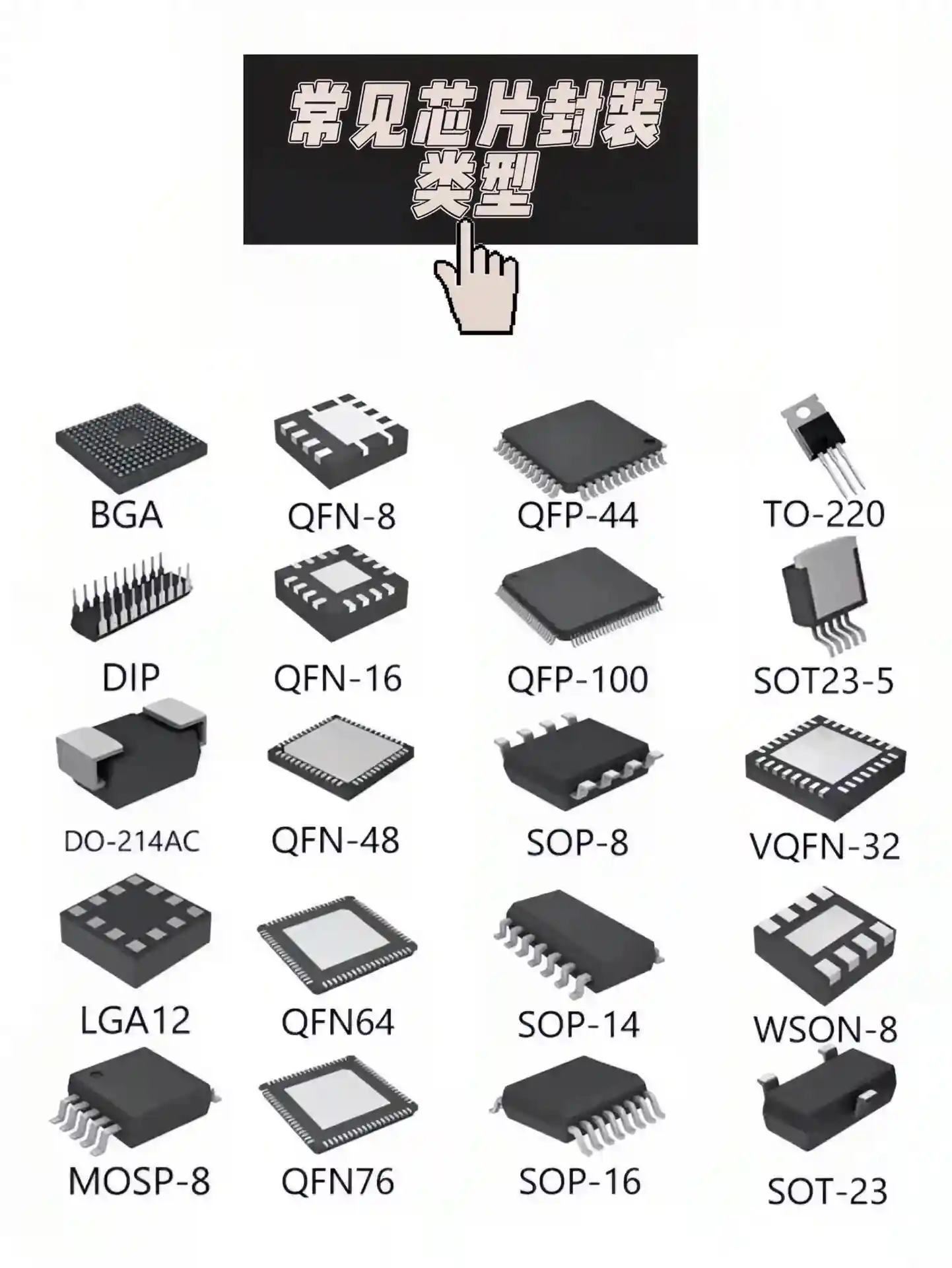
1. Follow IPC Standards (But Know When to Adapt)
The IPC-7351 standard provides guidelines for land patterns, but real-world designs often require adjustments:
Practical Tip:
2. Optimize Pad Geometry for Soldering
A. Passive Components (Resistors, Capacitors)
B. IC Packages (SOIC, QFP, BGA)
3. Thermal Management in Footprints
Thermal Pads:Use a grid of vias (e.g., 0.3mm diameter, 1mm spacing) under thermal pads for heat dissipation. Avoid via-in-pad unless your fab supports filled vias (risk of solder wicking).
4. Design for Manufacturing (DFM) Checks
A. Clearance Rules
B. Fiducial Marks & Tooling Holes: Include three global fiducials (1mm diameter, non-solder-masked) for pick-and-place alignment.
5. Future-Proofing for Miniaturization
A. Micro-BGAs and 01005 Passives
B. Flex/Rigid-Flex PCBs: Reinforced Pads: Add anchor points (teardrops) at flex-to-rigid transitions.
6. Footprint Validation Workflow
Conclusion
A robust footprint design ensures reliable assembly, reduces rework, and extends product life. By combining IPC standards with real-world DFM insights, engineers can avoid costly mistakes and adapt to evolving packaging trends. Need a footprint design review? Our engineering team offers free DFM audits—contact us today!
With 16 years of expertise in PCBA design, manufacturing, and service, KingshengPCBA is ready to help turn your ideas into reality. Feel free to contact us anytime to discuss your requirements and get a professional quotation.

Please send Email to kspcba@c-alley.com or call us through +86 13828766801 Or submit your inquiry by online form. Please fill out below form and attach your manufacturing files( PCB Gerber files and BOM List) if need quotation. We will contact you shortly.
 +86 13828766801
 kspcba@c-alley.com
 https://www.kingshengpcba.com/
 2/F, Building 6, Tangtou 3rd Industrial Zone, Tangtou Community, Shiyan Town, Baoan District, Shenzhen, China, 518108
We would also like to thank our customers for their trust and support. The company's outstanding achievements are mainly due to the loyalty of our customers, which also encourages and spurs our company to forge ahead.


