* On your first PCB Assembly order!
* Up to $300 discount
 C - A L L E Y
 Home | Events | PCB | About Us | News | Contact Us
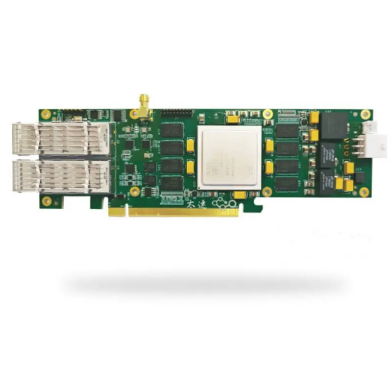
In the era of explosive growth in computing power from AI and data centers, server motherboards and accelerator cards are no longer traditional computer components, but rather the digital foundation supporting trillions of parameter models and massive data processing. The manufacturing complexity of these boards has approached the limits of industrial electronics manufacturing, with each step testing the manufacturer's technical depth and engineering capabilities.
I. Oversized Design: Challenges Starting from the Physical Dimension
Extremely Large Size and High Multilayer Board Structure:
Server motherboards often exceed 500mm in length, and accelerator cards are also trending towards full-height, full-length specifications. The increased physical size leads to an exponential increase in the difficulty of controlling the coefficient of thermal expansion (CTE) during reflow soldering. To accommodate high multilayer board designs with 20 or more layers, ultra-low loss materials (such as the MEGTRON series) must be used, and impedance continuity must be controlled through precise layer stack-up design to ensure the integrity of 112Gbps high-speed signals.
Large BGA Packaging and Micro-Pitch Arrays:
The number of BGA pins for CPUs/GPUs/XPUs has exceeded 2500 balls, with some accelerator chips even reaching 6000+ solder balls. Micro-pitch ball grid arrays of 0.8mm and below require solder paste printing accuracy controlled within ±15 micrometers. This necessitates processes such as laser stencil cutting and multi-stage verification using 3D SPI (solder paste inspection).
II. Power and Heat Dissipation: An Engineering Game of Energy Density
Hybrid Assembly of High-Power Power Supply Modules:
Single accelerator cards exceeding 1000W power is now commonplace, requiring the power supply section to integrate high-current VRMs, multi-phase digital PWM controllers, and power inductors. These modules often employ a hybrid design of "thick copper PCB + high-mass magnetic components," resulting in significant thermal mass differences during reflow soldering. The solution is to use "segmented reflow soldering profiles," independently controlling the temperature zones of components with different temperature requirements to avoid cold solder joints and thermal damage.
Mechanical Precision of Liquid Cooling Interfaces:
The mounting interface of Direct Liquid Cooling (DLC) modules requires extremely high flatness with the PCB (typically requiring a tolerance of <0.2mm). During manufacturing, CNC riveting of copper pillars is used at critical mechanical holes, and a flatness laser inspection process is added after SMT to ensure uniform pressure distribution during cold plate mounting and avoid signal breakage risks caused by PCB bending.
III. Assembly Process: Precision Manufacturing of Heavy-Duty Boards
Heavy-Duty Support Fixture System:
Traditional PCB conveyor tracks cannot support the assembly of boards weighing over 5kg. The production line needs customized carbon fiber support fixtures to provide uniform heat conduction in the reflow oven while preventing deformation caused by board sagging due to its own weight. The fixture design must also avoid bottom-mounted components and consider thermal stability under nitrogen reflow conditions.
Collaborative Assembly Process (CAP):
For three-section density distribution boards that simultaneously include a front-end high-speed connector, a large-size BGA chip in the middle, and a high-power inductor at the back, a "staged mounting and reflow" process is adopted: first, mechanical fasteners and bottom components are soldered; then, the main BGA is soldered after flipping the board over; finally, heat-sensitive components such as liquid cooling modules are manually assembled. The entire process requires tracking the board stress deformation data at each stage through an MES system to form a closed-loop process adjustment.
IV. Testing and Verification
Server-grade boards must pass:
*3D X-ray inspection: Layered scanning of hidden solder joints to identify voids and bridging defects in the BGA area.
*Thermal cycling stress testing: Simulating interconnect reliability under drastic temperature changes from -40℃ to 125℃.
*Vector network analysis: S-parameter testing of PCIe 5.0/6.0 and DDR5 channels to ensure signal attenuation is within budget.
Conclusion
The essence of manufacturing this type of "computing power base" is balancing the multi-dimensional constraints of electrical performance, mechanical strength, and thermal management at the millimeter scale. Only by deeply integrating materials science, precision mechanics, and process control can cutting-edge chip designs be transformed into reliable computing units. This is precisely the real barrier hidden behind the specifications in the competition for computing infrastructure.
With 16 years of expertise in PCBA design, manufacturing, and service, KingshengPCBA is ready to help turn your ideas into reality. Feel free to contact us anytime to discuss your requirements and get a professional quotation.

Please send Email to kspcba@c-alley.com or call us through +86 13828766801 Or submit your inquiry by online form. Please fill out below form and attach your manufacturing files( PCB Gerber files and BOM List) if need quotation. We will contact you shortly.
 +86 13828766801
 kspcba@c-alley.com
 https://www.kingshengpcba.com/
 2/F, Building 6, Tangtou 3rd Industrial Zone, Tangtou Community, Shiyan Town, Baoan District, Shenzhen, China, 518108
We would also like to thank our customers for their trust and support. The company's outstanding achievements are mainly due to the loyalty of our customers, which also encourages and spurs our company to forge ahead.


