* On your first PCB Assembly order!
* Up to $300 discount
 C - A L L E Y
 Home | Events | PCB | About Us | News | Contact Us
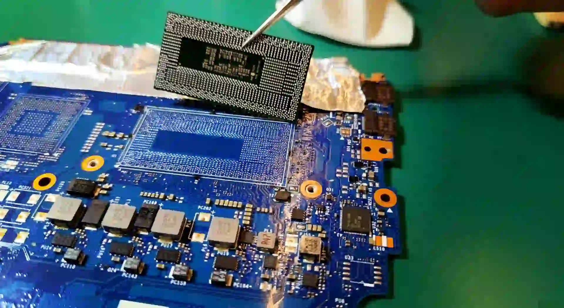
In modern PCBA manufacturing, BGAs are the backbone of high-performance electronics—powering smartphones, industrial controllers, and 5G base stations. But their dense, bottom-mounted solder balls make rework one of the trickiest tasks: a single misstep can ruin a high-value chip or damage the PCB, wasting time and materials. At [Your PCBA Brand], we’ve refined our BGA rework process to hit a 98%+ success rate. Here’s how we do it:
Essential Tools for Reliable BGA Rework
You can’t fix what you can’t control—and the right tools are non-negotiable:
.3-Zone BGA Rework Station: Our go-to tool features independent top/bottom heating to evenly warm the PCB and chip, avoiding thermal shock. The built-in optical alignment system ensures sub-10μm precision when repositioning BGAs, cutting down on offset-related failures.
Precision Reballing Kit: For damaged chips, we use laser-cut stencils matched to your BGA’s pitch, paired with high-purity solder balls and no-clean flux to ensure uniform, defect-free reballing.
Step-by-Step BGA Rework Process
Our standardized process leaves zero room for guesswork:
Pre-Rework Prep: First, we bake moisture-sensitive PCBs at 120°C for 10–20 hours (per IPC standards) to prevent delamination during heating. We also mark the BGA’s orientation to avoid misalignment later.
Controlled Removal: We load a custom temperature profile (optimized for your chip and PCB material) into the rework station. Once the solder melts, we gently lift the chip with a vacuum pen—no prying, to avoid damaging pads.
Clean & Prep: We use solder wick and a temperature-controlled iron to remove excess solder from the PCB pads, then clean with isopropyl alcohol to ensure a flat, contamination-free surface. For reballing, we clean the chip’s pads and align the stencil to apply fresh solder balls.
Precision Reattachment: Using the rework station’s optical alignment, we position the chip exactly over the pads, then run the pre-set reflow profile to melt the solder. We let the PCB cool slowly to avoid thermal stress.
Inspect & Validate: Finally, we perform X-ray inspection to check for voids or bridges, followed by a functional test to confirm the chip works as intended.
Pro Tips to Boost Rework Success Rate
Even with great tools, details make all the difference:
A)Customize Temperature Profiles: Generic profiles don’t work—we create unique curves for every BGA-PCB combo, balancing preheat, reflow, and cooling rates to avoid overheating components or causing solder defects.
B)Prioritize ESD Safety: 15% of BGA rework failures we’ve seen are due to static damage. Enforce strict ESD protocols for every rework task.
C)Clean Thoroughly: Residual flux or solder residue leads to cold joints. We use ultrasonic cleaners for chip pads and lint-free wipes for PCBs to ensure a perfect bond.
D)Train Your Team: Our rework technicians go through 100+ hours of hands-on training and quarterly certification. Well-trained staff catch small issues before they become big problems.
E)Track & Iterate:We log every rework task—temperature profiles, chip types, success rates—to refine our process over time. This data-driven approach has helped us cut failure rates by 40% in the last year.
Partner With Experts for Stress-Free BGA Rework
BGA rework isn’t a DIY task. Our team’s expertise and standardized process mean we can rescue high-value PCBs that would otherwise be scrapped, saving you time and money.
If you’re struggling with BGA rework challenges, drop us a line—we’re here to help you get the highest success rate possible.
ESD Protection Gear: Static discharge is BGA’s silent killer. We require ESD wristbands, grounded workbenches, and anti-static bags for all rework tasks to protect sensitive chips.
Inspection Tools: Post-rework, we use X-ray scanners to check hidden solder joints and high-magnification microscopes for surface defects, ensuring no issues slip through the cracks.
With 16 years of expertise in PCBA design, manufacturing, and service, KingshengPCBA is ready to help turn your ideas into reality. Feel free to contact us anytime to discuss your requirements and get a professional quotation.

Please send Email to kspcba@c-alley.com or call us through +86 13828766801 Or submit your inquiry by online form. Please fill out below form and attach your manufacturing files( PCB Gerber files and BOM List) if need quotation. We will contact you shortly.
 +86 13828766801
 kspcba@c-alley.com
 https://www.kingshengpcba.com/
 2/F, Building 6, Tangtou 3rd Industrial Zone, Tangtou Community, Shiyan Town, Baoan District, Shenzhen, China, 518108
We would also like to thank our customers for their trust and support. The company's outstanding achievements are mainly due to the loyalty of our customers, which also encourages and spurs our company to forge ahead.


