* On your first PCB Assembly order!
* Up to $300 discount
 C - A L L E Y
 Home | Events | PCB | About Us | News | Contact Us
In the age of 5G, high-speed computing, and IoT, signal integrity (SI) is non-negotiable for reliable electronic performance. Even minor signal distortion can trigger data errors, timing mismatches, or system crashes. For PCBA manufacturers like us, one of the most impactful yet overlooked drivers of SI is multilayer PCB stack-up design. Here’s how stack-up choices directly influence signal quality, and key optimizations to build for SI success.
1. Layer Arrangement: The Foundation of SI
The order of signal, power, and ground layers defines SI from the start.
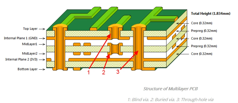
A) Pair every signal layer with a solid ground or power plane: This provides a low-impedance return path, minimizing loop area and cutting electromagnetic interference (EMI). A 4-layer stack-up like Top Signal → Ground → Power → Bottom Signal is a gold standard for balancing cost and SI, shielding signals and reducing crosstalk.
B)Avoid adjacent signal layers: Fast-changing traces in adjacent layers induce unwanted coupling, a top cause of SI failures in high-speed circuits (200MHz+).
2. Impedance Control: Stop Signal Reflection
Impedance mismatches cause reflection, overshoot, and ringing—critical threats to SI. Stack-up design is the backbone of precise impedance control:
A)Adjust trace width, dielectric thickness, and substrate material to hit targets (e.g., 50Ω for single-ended signals, 100Ω for differential pairs like PCIe or LVDS).
B)Our engineers use tools like the Polar SI6000 to simulate impedance during stack-up design, validating every trace meets your specs before manufacturing begins.
3. Substrate Materials: Minimize Signal Loss
The right substrate stabilizes signal propagation and reduces attenuation, especially at high frequencies:
A)For high-speed designs, opt for low-dissipation-factor (tanδ) materials like Panasonic Megtron6 or Rogers RO4350B. These reduce signal loss at GHz frequencies, ensuring signals retain quality over long traces.
B)Standard FR-4 works for low-speed circuits, but its higher tanδ leads to noticeable signal degradation at speeds above 1GHz.
4. Power & Ground Planes: Stabilize Signals from the Source
Stable power and ground are inseparable from SI:
A)Place power and ground layers adjacent to each other: They act as high-frequency capacitors, delivering instantaneous current to fast-switching ICs and reducing power noise that distorts signals.
B)Avoid over-dividing power planes: Fragmented planes break signal return paths, introducing unwanted noise. Our team balances power distribution needs with SI, placing decoupling capacitors near high-speed ICs to further stabilize signals.
Why Partner with a PCBA Expert for Stack-Up Design
A well-optimized stack-up eliminates post-manufacturing debugging and boosts long-term reliability.As a full-service PCBA manufacturer, we partner with you from the early design phase to tailor stack-up to your circuit’s speed, power, and budget needs. Whether you’re building a 4-layer industrial controller or a 12-layer 5G baseband board, our engineering expertise ensures your stack-up is built for uncompromised SI.
Ready to optimize your PCB stack-up for signal integrity? Reach out to C-alley our team today for a free, personalized design consultation.
With 16 years of expertise in PCBA design, manufacturing, and service, KingshengPCBA is ready to help turn your ideas into reality. Feel free to contact us anytime to discuss your requirements and get a professional quotation.

Please send Email to kspcba@c-alley.com or call us through +86 13828766801 Or submit your inquiry by online form. Please fill out below form and attach your manufacturing files( PCB Gerber files and BOM List) if need quotation. We will contact you shortly.
 +86 13828766801
 kspcba@c-alley.com
 https://www.kingshengpcba.com/
 2/F, Building 6, Tangtou 3rd Industrial Zone, Tangtou Community, Shiyan Town, Baoan District, Shenzhen, China, 518108
We would also like to thank our customers for their trust and support. The company's outstanding achievements are mainly due to the loyalty of our customers, which also encourages and spurs our company to forge ahead.


