* On your first PCB Assembly order!
* Up to $300 discount
 C - A L L E Y
 Home | Events | PCB | About Us | News | Contact Us
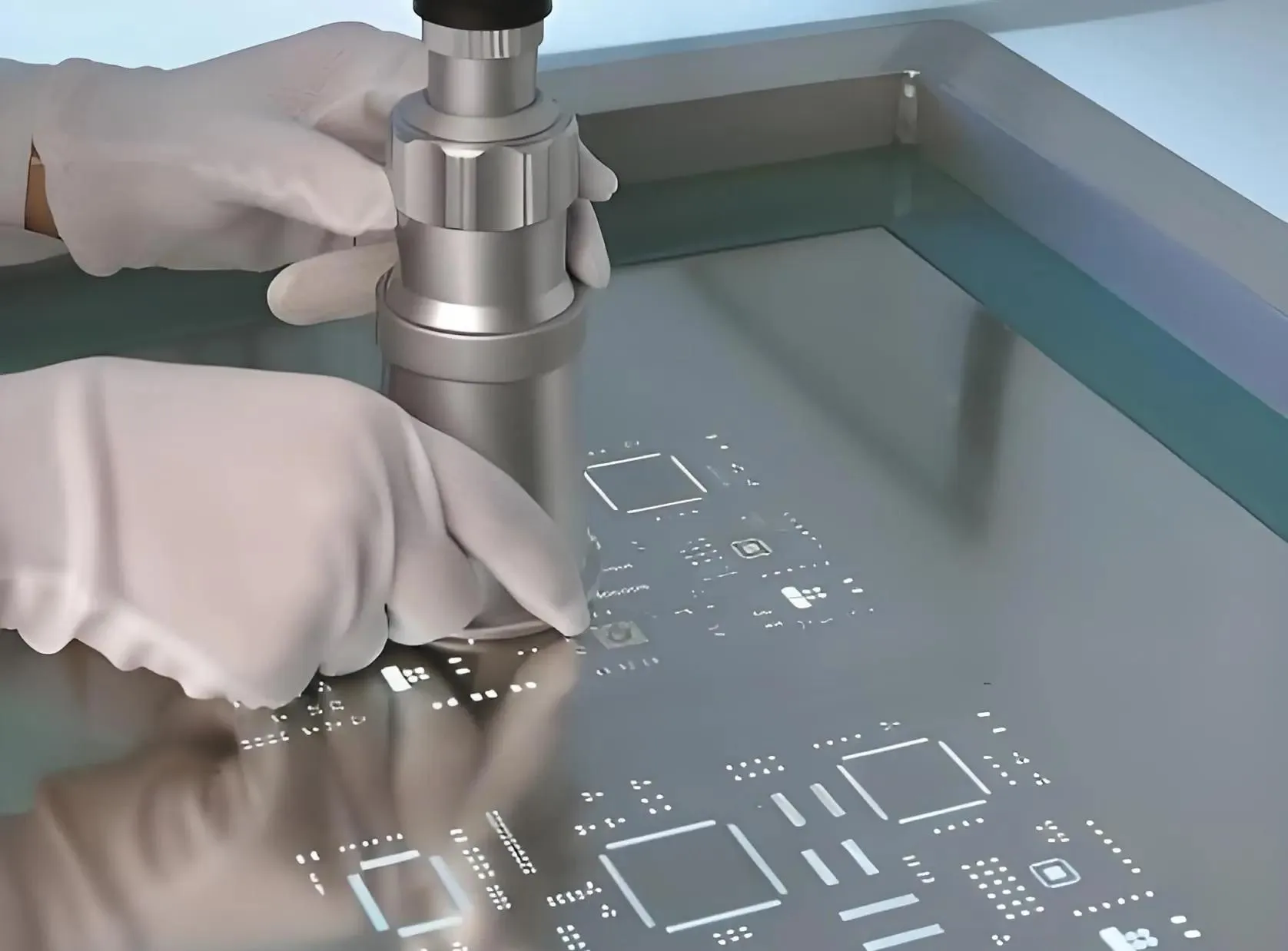
In the fast-paced world of PCBA manufacturing, SMT placement yield directly impacts production costs, delivery timelines, and product reliability. Even small defects like solder balls, bridges, or tombstoning can lead to costly reworks or field failures. While many factors influence yield, one often-underappreciated hero is the stencil. A well-designed stencil with optimized apertures ensures precise solder paste deposition—the foundation of robust, defect-free soldering. As a leading PCBA manufacturer, we’ve refined our stencil strategies over years of practice, helping clients cut defect rates by 80% or more. Here’s how we do it.
1. Pick the Right Material & Thickness for Your Components
The stencil’s material and thickness set the baseline for solder paste control. We exclusively use laser-cut stainless steel stencils with electropolished holes for smooth, consistent paste release.
Thickness is tailored to component types:
A: For tiny 0201 components: 0.10–0.12mm stencils to avoid excess paste and tombstoning (we once reduced a wearable device’s tombstoning rate from 2.3% to 0.15% with this adjustment).
B: For standard 0402/0603 parts: 0.12–0.15mm stencils to balance solder volume and connection strength.
C: For BGAs or high-pin-count ICs: 0.15–0.20mm stencils paired with a 1:0.9 aperture ratio to ensure sufficient solder for reliable joints while preventing bridging.
2. Optimize Aperture Shape & Size to Defeat Common Defects
Aperture design is where we target defects at the source:
A: Solder ball prevention: For small resistors or capacitors, we reduce the aperture area under the component body by 10–20%. This limits excess paste that can squeeze out during placement and form unwanted solder balls.
B: Tombstoning elimination: For 0402 and smaller components, we strictly use symmetric apertures to ensure equal solder volume on both pads, balancing wetting forces and stopping components from tipping.
C: BGA reliability: For fine-pitch BGAs, we use offset or truncated apertures to avoid pad bridging while maintaining enough solder volume for strong joints. For MOSFETs with bottom pads, we adopt a centered cross-shaped aperture (60% of pad area) to control solder flow and avoid shorts.
3. Customize Apertures for Special Components
Unique parts demand tailored solutions:
A: For Micro USB connectors: Widen outer conductive pads by 0.2mm and use 70% aperture size for inner pins to enhance connection stability without bridging.
B: For large ground pads: Split apertures into a grid pattern to reduce solder pull and ensure uniform paste deposition, avoiding voids under heavy components.
C: We also enforce a 0.25mm minimum gap between adjacent apertures to eliminate cross-contamination and bridging risks.
4. Maintain Stencil Performance Long-Term
Even the best stencil won’t perform well without proper care:
A: Auto-clean stencils after every 50–100 boards, followed by manual deep cleaning with alcohol and a dry wipe shift to avoid solvent residue that harms paste flow.
B: Regularly test stencil tension (38–60N) to keep it flat and aligned with PCBs, preventing uneven paste deposition.
C: Store stencils in dust-free, moisture-proof cases to extend their lifespan.
Our Stencil Design Service: Yield Improvement From the Start
As part of our DFM (Design for Manufacturability) process, we review your PCB design and BOM to recommend stencil optimizations before production begins. Our team combines decades of engineering experience with AOI defect data to refine apertures, ensuring your stencil is tailored to your unique design. We also provide post-production stencil performance reports to help you iterate for even better yield in future runs.
Stencil design isn’t an afterthought—it’s the first step to high-yield SMT production. By investing in optimized stencils, you cut rework costs, speed up time-to-market, and deliver more reliable products. Ready to boost your SMT yield? Reach out to our team today for a free stencil design consultation.
With 16 years of expertise in PCBA design, manufacturing, and service, KingshengPCBA is ready to help turn your ideas into reality. Feel free to contact us anytime to discuss your requirements and get a professional quotation.

Please send Email to kspcba@c-alley.com or call us through +86 13828766801 Or submit your inquiry by online form. Please fill out below form and attach your manufacturing files( PCB Gerber files and BOM List) if need quotation. We will contact you shortly.
 +86 13828766801
 kspcba@c-alley.com
 https://www.kingshengpcba.com/
 2/F, Building 6, Tangtou 3rd Industrial Zone, Tangtou Community, Shiyan Town, Baoan District, Shenzhen, China, 518108
We would also like to thank our customers for their trust and support. The company's outstanding achievements are mainly due to the loyalty of our customers, which also encourages and spurs our company to forge ahead.


