* On your first PCB Assembly order!
* Up to $300 discount
 C - A L L E Y
 Home | Events | PCB | About Us | News | Contact Us
I. Engineering Principles for Multilayer PCB Stack-Up Planning
1.1 Return Path Integrity and Forbidden Areas for Partitioning
Key Understanding: The return current of a high-speed signal does not flow through "ground" but through the reference plane with the lowest path impedance. For signals above 100 MHz, the return current concentrates within a 3W range directly below the signal line on the reference plane.
Design Rules:
* Any crossing of a split (power plane split, ground plane slot) will cause a sudden change in the return path, resulting in common-mode radiation.
* When critical signal lines (clock, differential pairs) cross a split gap, stitching capacitors (typically 100 nF) must be placed on both sides of the gap.
*When a power plane is used as a reference plane, it is necessary to ensure that decoupling capacitors are present within 20 mils below the signal.
1.2 Quantitative Criteria for Stack-Up Symmetry
The amount of warpage caused by an asymmetric layer stack can be estimated using the following empirical formula:
Warpage ≈ α × ΔCTE × ΔT × (L² / h)
where ΔCTE is the difference in the coefficient of thermal expansion in the xy direction. Typical FR-4, ΔCTE can reach 13-18 ppm/°C.
Engineering Practices:
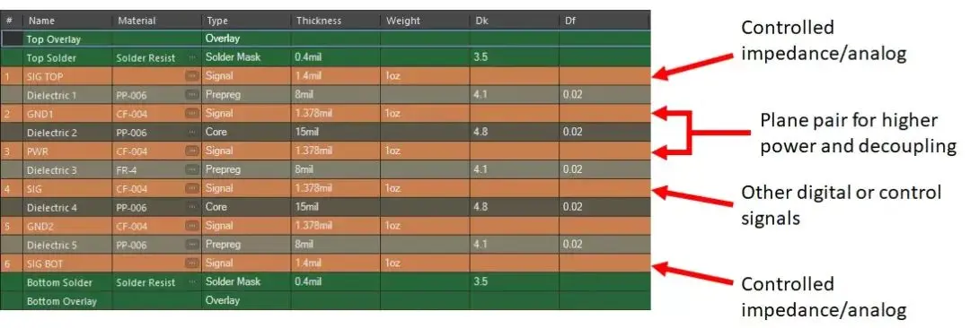
*Standard 6-layer structure: Top-Gnd-Sig-Pwr-Sig-Bottom (asymmetric, with warpage risk)
*Improved structure: Top-Gnd-Sig-Pwr-Gnd-Bottom (adding a ground layer to improve symmetry)
*Optimal structure: Top-Gnd-Sig1-Pwr/Gnd-Sig2-Gnd-Bottom (completely symmetric)
II. Physical Essence and Process Compensation of Impedance Calculation
2.1 Accuracy Boundary of Transmission Line Model
Commonly used microstrip line impedance formula:
Z₀ = (87/√(ε_eff+1.41)) × ln(5.98H/(0.8W+T))
Practical engineering considerations include:
*Copper foil roughness effect: At 10 GHz, HVLP copper foil (Rz=1.2μm) exhibits 30% lower loss compared to STD copper foil (Rz=3.6μm).
*Solder mask impact: LPI solder mask (ε_r=3.2) can reduce the impedance of surface microstrip lines by 2-3Ω.
*Fiber weave effect: 1078 glass weave (fiber bundle spacing of 112μm) can cause periodic impedance variations of ±5%.
2.2 Common-Mode and Differential-Mode Coupling in Differential Impedance
Key findings: The odd-mode impedance (Z_odd) and even-mode impedance (Z_even) of a differential pair satisfy the following relationships:
Z_diff = 2 × Z_odd
Z_comm = Z_even / 2
When the line spacing S < 2W, coupling coefficient k > 0.3, the coupling differential line model must be used for calculations.
Design Data Table:
| Application Scenario | Target Impedance (Ω) | Line Width (mil) | Spacing (mil) | Dielectric Thickness (mil) |
| USB 2.0 | 90±7% | 5.5 | 8.5 | 4.2 |
| PCIe Gen3 | 85±5% | 4.0 | 8.0 | 3.5 |
| DDR4 | 40±10% | 4.5 | - | 3.0 |
III. Material Performance: Frequency Variation Characteristics and Selection Matrix
3.1 Frequency Response of Dielectric Constant and Loss Tangent
Typical variations of FR-4 material within the 1MHz-10GHz range are as follows:
*Dk (ε_r): Decreases from 4.7 (1MHz) to 4.3 (10GHz), with a change rate of approximately 8.5%.
*Df (tanδ): Increases from 0.020 (1MHz) to 0.025 (10GHz).
High-Speed Material Comparison Matrix:
| Material Type | Dk@1GHz | Df@1GHz | Cost Factor | Applicable Frequency Range |
| FR-4 (Tg150) | 4.3 | 0.018 | 1.0 | < 2GHz |
| Megtron 6 | 3.6 | 0.002 | 8.0 | < 25GHz |
| Rogers 4350B | 3.48 | 0.0037 | 12.0 | < 30GHz |
| Teflon (PTFE) | 2.2 | 0.0009 | 25.0 | < 77GHz |
3.2 Quantitative Analysis of Glass Weave Effect
For 1080 glass cloth (warp and weft density: 60×47 threads/inch):
*Fiberglass bundle width: 3.5mil
*Opening area width: 2.8mil
*Dk difference: Fiberglass region 4.7 vs Resin region 3.9
Solutions:
1. Employ flat fiberglass cloth (such as 1067) to ensure Dk fluctuation is less than ±2%.
2. Use an opening design, but be aware of a 20% reduction in mechanical strength.
3. Rotate the trace angle 7-15° to disrupt periodic resonance.
3.3 Skin Effect Depth and Surface Roughness of Copper Foil
Skin effect depth formula: δ = 66/√f (μm, f in GHz)
For 10GHz signal:
*Skin effect depth is only 0.66μm.
*The actual conductive thickness of the copper foil is only 1-2μm.
*The depth of rough peaks and valleys is the main limiting factor for the equivalent conductive cross-section.
IV. Experimental Verification and Process Control Points
4.1 Accuracy calibration of TDR measurement system
* Probe tip parasitic capacitance should be less than 0.1 pF.
* Rise time selection: t_rise < 0.5 × electrical length (For 3-inch cable, t_rise < 35ps)
*Impedance fluctuation criterion: ΔZ > ±5% within a continuous 1 inch must be marked as a risk point.
4.2 Factory Process Capability Matrix (Typical Values)
| Parameter | Conventional Process | High-Precision Process | Extreme Process |
| Line Width Control | ±15% | ±8% | ±3% |
| Dielectric Thickness | ±10% | ±6% | ±3% |
| Copper Thickness (1oz) | ±15% | ±10% | ±5% |
| Etch Factor | 2:1 | 3:1 | 5:1 |
| Dk Control | ±5% | ±3% | ±1% |
4.3 Design Redundancy Recommendations
* Impedance Line Width Margin: Target value must meet specifications within ±10%.
*Critical networks: Reserve locations for π-type matching resistors (0 Ω/22 Ω/33 Ω).
*Sensitive Signals: Add grounded shielding vias on both sides with a spacing of less than λ/20.
V. Emerging Trends: Heterogeneous Integration and 3D Interconnects
1. Hybrid Dielectric Stacking: Employ M6 high-speed material for the surface layer and FR-4 for the inner layers to balance cost and performance.
2. Localized Copper Foil Thickening: Utilize 2oz copper in specific areas of the power supply path to reduce DC voltage drop while managing costs.
3. Vertical Interconnects: Optimize vertical interconnect density in 20+ layer boards through a hybrid approach using stacked vias and staggered vias.
True professional design is not simply applying formulas; rather, it involves understanding the physical meaning behind each parameter and finding the optimal balance among cost, manufacturability, and performance.
Each optimization of the impedance profile represents a precise mapping from electromagnetic field theory to engineering practice.
With 16 years of expertise in PCBA design, manufacturing, and service, KingshengPCBA is ready to help turn your ideas into reality. Feel free to contact us anytime to discuss your requirements and get a professional quotation.

Please send Email to kspcba@c-alley.com or call us through +86 13828766801 Or submit your inquiry by online form. Please fill out below form and attach your manufacturing files( PCB Gerber files and BOM List) if need quotation. We will contact you shortly.
 +86 13828766801
 kspcba@c-alley.com
 https://www.kingshengpcba.com/
 2/F, Building 6, Tangtou 3rd Industrial Zone, Tangtou Community, Shiyan Town, Baoan District, Shenzhen, China, 518108
We would also like to thank our customers for their trust and support. The company's outstanding achievements are mainly due to the loyalty of our customers, which also encourages and spurs our company to forge ahead.


