* On your first PCB Assembly order!
* Up to $300 discount
 C - A L L E Y
 Home | Events | PCB | About Us | News | Contact Us
In PCBA design, adding extra blank space along the board edges—known as process edges or manufacturing allowances—isn't wasted real estate. It's a critical Design for Manufacturability (DFM) practice that bridges your circuit design and successful mass production. This guide explains why process edges are essential, detailing their role in automated assembly, testing, and overall product reliability.
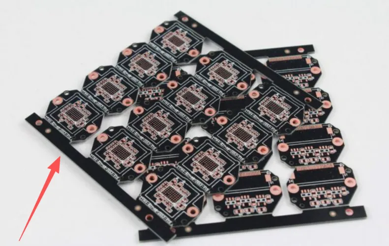
What Are PCBA Process Edges?
Process edges are elongated, blank zones reserved along the periphery of a PCB panel or individual board. This area remains free of components, traces, or pads. According to standards like IPC-A-610, a single process edge should typically be at least 5mm wide (8mm or more for high-precision boards), with smooth, flush peripheries to prevent jamming in equipment rails.
Core Purpose: They serve as a mechanical handling area for automated equipment—SMT pick-and-place machines, wave soldering conveyors, and testing fixtures—ensuring stable gripping, transport, and positioning throughout production.
The 3 Critical Benefits of Designing Process Edges
Incorporating process edges is a proactive strategy to prevent production failures and cost overruns. Here are their three primary benefits:
1. Enables Stable Automated Assembly (SMT & Wave Soldering)
Automated production lines rely on conveyor rails to transport boards. Process edges provide the necessary clearance for these grippers. Without them, boards can jam, shift, or be rejected by the machine, causing line stoppages and placement inaccuracies. For small or irregularly shaped PCBs, process edges effectively extend the board to meet the equipment's minimum size requirement.
2. Protects Components from Mechanical Damage
Components placed too close to the board edge risk collision with the nozzles of SMT placement machines or fixtures during wave soldering. A dedicated process edge creates a safe “keep-out zone,” preventing costly damage to components and ensuring a smooth, uninterrupted production flow.
3. Provides Space for Critical Features: Fiducials & Testing
Fiducial Marks (Mark Points): These optical alignment targets for pick-and-place machines require a 3mm clearance from any other feature. Process edges offer the ideal, unobstructed location for them. Testing Fixture Support: During ICT (In-Circuit Test) and FCT (Functional Test), fixtures use the process edges to securely clamp the board, ensuring test probes make accurate contact. This improves test reliability and yield.
How to Remove Process Edges: Methods & Best Practices
After assembly, process edges must be cleanly removed. The method impacts final board quality and cost.
| Method | Process | Best For | Key Considerations |
|---|---|---|---|
| Routing/Milling | High-speed CNC router cuts along the edge. | High-volume, high-reliability products; complex board shapes. | Pros: Smoothest edge, high precision, minimal stress. Cons: Higher equipment cost. |
| V-Scoring/Separation | Board is separated along pre-cut V-grooves. | High-volume, rectangular panels with straight edges. | Pros: Fast, low-cost, dust-free. Cons: Limited to straight lines; requires precise V-groove design. |
| Manual Breakaway | Edges are snapped off by hand or with pliers. | Low-volume prototypes, simple boards with breakaway tabs. | Pros: Zero equipment cost, maximum flexibility. Cons: Risk of board stress, cracks, or uneven edges. Use breakaway tabs (mouse bites) to localize stress. |
Design Tip: If using manual removal, design the connection between the process edge and main board with breakaway tabs (a series of small drilled holes) to concentrate stress and protect the main board.
Conclusion: A Foundational DFM Principle
Process edge design is a fundamental DFM (Design for Manufacturability) principle. It is a small design consideration with an outsized impact on production yield, equipment compatibility, and final product quality.
Before finalizing your board layout, always ask:
Have I reserved sufficient, clear process edges (≥5mm) on opposite sides for conveyor handling?
Are my fiducial marks placed within this area, with proper clearance?
Have I selected an appropriate removal method (routing, V-scoring, breakaway) and designed the panel accordingly?
Remember: The most elegant circuit design can fail in production without thoughtful manufacturing allowances. A well-designed process edge is a low-cost investment that guarantees your design can be built reliably, efficiently, and at scale.
With 16 years of expertise in PCBA design, manufacturing, and service, KingshengPCBA is ready to help turn your ideas into reality. Feel free to contact us anytime to discuss your requirements and get a professional quotation.

Please send Email to kspcba@c-alley.com or call us through +86 13828766801 Or submit your inquiry by online form. Please fill out below form and attach your manufacturing files( PCB Gerber files and BOM List) if need quotation. We will contact you shortly.
 +86 13828766801
 kspcba@c-alley.com
 https://www.kingshengpcba.com/
 2/F, Building 6, Tangtou 3rd Industrial Zone, Tangtou Community, Shiyan Town, Baoan District, Shenzhen, China, 518108
We would also like to thank our customers for their trust and support. The company's outstanding achievements are mainly due to the loyalty of our customers, which also encourages and spurs our company to forge ahead.


