* On your first PCB Assembly order!
* Up to $300 discount
 C - A L L E Y
 Home | Events | PCB | About Us | News | Contact Us
In the intricate world of PCB design, layout constraint management is the cornerstone of success. Moving beyond a generic “one-size-fits-all” approach to design rules is critical for creating boards that are not only electrically robust but also manufacturable and reliable. This guide delves into why precise constraint management is non-negotiable in modern electronics and how to implement it effectively.

Why PCB Layout Constraint Management is Crucial Today
Thirty years ago, PCB designs had more tolerance. Today, with higher speeds, denser components, and stricter EMI/EMC requirements, every micron counts. Layout constraints—governing trace spacing, width, component placement, and more—are the blueprint that ensures a design transitions from concept to a functional, producible product. Neglecting them introduces risks in signal integrity, power integrity, and manufacturability.
Key Electrical Considerations in Constraint Management
Precise design rules are paramount for electrical performance. Here are the primary factors your constraint manager must address:
1. Power Integrity & Current Carrying Capacity
High-current traces require increased trace widths to prevent overheating and voltage drop. Constraint rules automatically enforce these widths, eliminating manual errors.
2. Controlled Impedance & Signal Integrity
For high-speed signals (e.g., DDR, PCIe, USB), maintaining precise impedance is essential. Rules must specify trace width, layer stackup, and spacing relative to reference planes to minimize reflections and ensure clean signal transmission.
3. Timing & Length Matching
Critical parallel buses (e.g., between a processor and memory) require trace length matching and specific routing topologies. Constraint managers allow you to set target lengths and tolerances, ensuring signals arrive synchronously.
4. EMI/EMC Control
To mitigate electromagnetic interference, constraints can enforce shielding techniques. This includes specifying ground plane return paths, limiting parallel run lengths for sensitive traces, and managing via stitching.
Essential Manufacturing Constraints for DFM Success
A perfect electrical design can fail in production if manufacturing constraints are ignored. Design for Manufacturability (DFM) rules bridge this gap:
1. Component Spacing & Assembly
Rules must ensure adequate clearance for automated pick-and-place machines and allow space for manual rework. This includes chip component spacing, orientation, and keep-out areas.
2. Solderability & Thermal Relief
To prevent tombstoning or cold solder joints, constraints govern solder mask expansion, pad sizes, and the use of thermal relief connections for pins connected to large copper pours, ensuring even heat distribution during reflow.
3. Testability & Accessibility
Designs must include access for flying probe test points and allow technicians to reach connectors, switches, and adjustment components. Constraints define keep-out zones and test point requirements.
The High Cost of Poor Constraint Management
Relying on defaults or manual oversight leads to predictable and costly problems:
Rework & Delays: Electrical failures (crosstalk, EMI) or DFM violations discovered post-layout necessitate extensive redesign.
Manufacturing Defects: Inadequate clearances cause solder bridges; improper thermal design leads to poor yields.
Inconsistent Design Quality: Without a central constraint manager, team members may apply rules inconsistently, compromising design reuse and reliability.
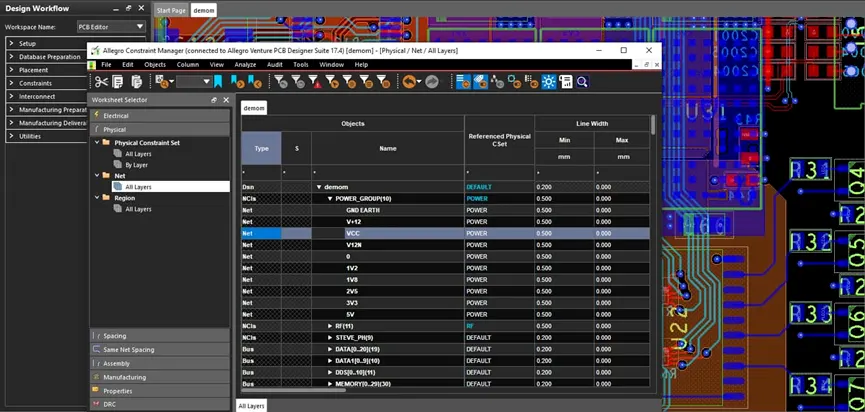
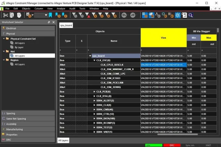
Leveraging Modern Constraint Management Systems: A Cadence Allegro Example
Modern EDA tools like Cadence Allegro PCB Designer have transformed constraint management from a chore into a strategic advantage. Its Constraint Manager offers features critical for efficiency:
Spreadsheet-like Interface: Enables bulk editing, copy-paste, and powerful search, making rule entry intuitive.
Hierarchical Rule Setting: Apply rules globally, by net class (e.g., “DDR4_CLK”), or to individual nets, providing granular control.
Comprehensive Rule Types: Manage everything from physical spacing and via selection to complex electrical rules for impedance, propagation delay, and differential pairs.
Schematic-Driven Layout (SDL): Define constraints in the schematic and let them drive the layout process, ensuring intent is preserved.
Best Practices for Effective Constraint Setup
Start Early: Define constraint templates during the schematic phase.
Collaborate: Involve both PCB layout engineers and signal integrity experts in rule creation.
Leverage Templates: Create and reuse rule sets for common technologies (e.g., DDR4, PCIe, RF) to ensure consistency across projects.
Validate Continuously: Use the tool’s real-time DRC (Design Rule Check) to catch violations during layout, not after.
Conclusion
Mastering PCB layout constraint management is no longer optional; it’s a fundamental skill for delivering high-quality, high-yield electronic products. By moving from ad-hoc adjustments to a rule-driven methodology, teams can dramatically reduce errors, improve performance, and accelerate time-to-market.
Ready to implement professional-grade constraint management in your designs?
Explore advanced resources or training, such as specialized courses on rule-driven PCB design, to systematically harness the full power of your EDA tools and elevate your design capabilities.
With 16 years of expertise in PCBA design, manufacturing, and service, KingshengPCBA is ready to help turn your ideas into reality. Feel free to contact us anytime to discuss your requirements and get a professional quotation.

Please send Email to kspcba@c-alley.com or call us through +86 13828766801 Or submit your inquiry by online form. Please fill out below form and attach your manufacturing files( PCB Gerber files and BOM List) if need quotation. We will contact you shortly.
 +86 13828766801
 kspcba@c-alley.com
 https://www.kingshengpcba.com/
 2/F, Building 6, Tangtou 3rd Industrial Zone, Tangtou Community, Shiyan Town, Baoan District, Shenzhen, China, 518108
We would also like to thank our customers for their trust and support. The company's outstanding achievements are mainly due to the loyalty of our customers, which also encourages and spurs our company to forge ahead.


