* On your first PCB Assembly order!
* Up to $300 discount
 C - A L L E Y
 Home | Events | PCB | About Us | News | Contact Us
In the field of electronics manufacturing, PCB and PCBA are two extremely important concepts, yet many people have a rather vague understanding of them and often confuse the two. Today, we shall delve into what exactly PCB and PCBA are, and examine the distinctions and connections between them.
I. PCB (Printed Circuit Board)
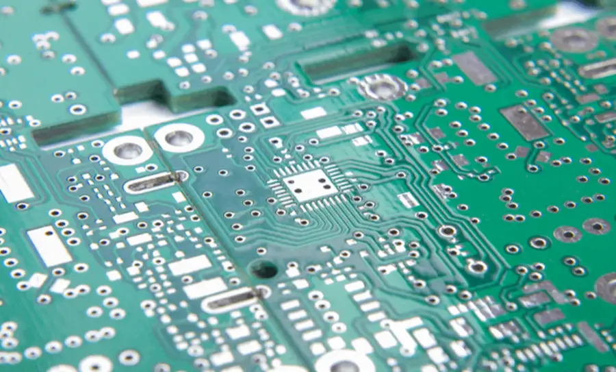
PCB, or Printed Circuit Board, is also known as a circuit board or PC board. It serves as the structural support for electronic components and the medium for electrical connections between them.
Typically crafted from insulating materials into a flat plate, PCBs feature conductive traces and connection points meticulously laid out according to the requirements of the electronic components. Its manufacturing process resembles a precision craftsmanship performance:
1. Substrate Preparation: Selecting suitable base materials, commonly FR4 (a flame-retardant glass fibre reinforced epoxy resin). For high-frequency applications, materials like PTFE are employed.
2. Pattern Exposure: Using a negative circuit pattern on film, an exposure unit projects the non-circuit areas onto the copper foil substrate. This step resembles sketching a precise blueprint onto blank paper.
3. Conductive Material Printing and Etching: Unwanted copper foil is removed through chemical etching, leaving only the required copper traces to form conductive pathways. This process resembles a sculptor meticulously carving away excess material to reveal the essence.
4. Drilling: Holes are drilled to connect signals across PCB layers, serving as conduits for signal transmission.
5. Soldering (and subsequent surface treatments): Surface treatments are applied, such as processing copper pads not covered by solder resist to prevent oxidation and enhance solderability. Operations like solder resist printing are also performed.
II. PCB's widespread adoption in the electronics industry stems from its distinctive advantages:
1. High wiring density, compact size, and lightweight: This strongly supports the miniaturisation of electronic products, enabling devices to integrate more functions within limited space. For instance, the internal space of everyday smartphones is highly constrained; this PCB characteristic allows electronic components to be densely arranged, achieving multifunctionality.
2. High reproducibility and stability: Enabling mass production ensures consistent product replication and uniformity. This significantly reduces assembly errors associated with cable routing, while modular design further minimises maintenance, debugging, and inspection times. Computer motherboards exemplify this: standardised PCB production yields large quantities of stable, specification-compliant boards, simplifying subsequent assembly and servicing.
3. Automated production capability: PCB and PCBA manufacturing is now almost entirely automated. This not only reduces labour costs and operational errors but also substantially increases labour productivity. It facilitates lower product pricing and promotes wider adoption. On automated production lines, machinery executes each manufacturing step with precision, ensuring product quality while accelerating production speed.
III. PCBA (Printed Circuit Board Assembly) — Printed Circuit Board Assembly
PCBA, or Printed Circuit Board Assembly, represents further processing undertaken on the basis of PCBs. The PCBA manufacturing process involves subjecting blank PCB boards to a series of complex procedures, ultimately yielding a finished circuit board with specific functionalities. The manufacturing workflow is as follows:
1. PCB Design: Utilising EDA software (such as Altium Designer or KiCad) to design circuit diagrams and PCB layouts, defining component placement, routing rules, and layer stack-up. This step constitutes the critical foundation of PCBA production, akin to architectural blueprints determining the trajectory of the entire subsequent project.
2. Component Procurement: Electronic components are sourced according to the design documentation (Bill of Materials, BOM), ensuring specifications, models, and quality meet design requirements.
3. Surface Mount Technology (SMT) Assembly:
- Solder Paste Printing: Solder paste is applied to the PCB pads via a stencil, preparing the surface for subsequent component placement.
- Placement: Utilising placement machines to precisely position components onto the PCB. These machines function like precision robots, rapidly and accurately placing minute components into designated locations.
- Reflow Soldering: Heating the PCB to high temperatures melts the solder paste, firmly securing components to the PCB and completing electrical connections.
4. THT Through-Hole Assembly (for components unsuitable for SMT): Through-hole technology (THT) is employed for components such as large capacitors and connectors, typically soldered via wave soldering or manual soldering. In wave soldering, the PCB passes through a wave of molten solder to complete component attachment; manual soldering is used for special cases or small-batch production.
5. Inspection and Testing:
- AOI Inspection: Automated Optical Inspection examines soldering quality and component placement, swiftly identifying obvious soldering defects and placement errors.
- ICT Testing: In-Circuit Testing verifies circuit functionality, assessing the electrical performance of all components on the PCB.
- Functional Testing: Simulates real-world operating conditions to comprehensively evaluate the PCBA's overall performance, ensuring stable operation in practical applications.
6. Cleaning and Protection:
Residual flux and contaminants from the soldering process are removed through cleaning. A conformal coating (providing moisture, dust, and corrosion resistance) is then applied to enhance the PCBA's reliability and service life.
7. Packaging and Delivery: PCBA is packaged using anti-static materials before being delivered to the customer or proceeding to the next assembly stage, ensuring the product remains undamaged during transportation and storage.
PCBA plays a central role in electronic products, forming the core component of virtually all electronic devices. Examples include the mainboard in smartphones, graphics cards in computers, and automotive electronic control systems – the functionality of these products relies entirely on the stable operation of PCBA.
IV. Distinctions Between PCB and PCBA
1. Visual Aspects
- PCB: A standalone board featuring only circuitry without any components, presenting a clean and uncluttered appearance.
- PCBA: A board with various components such as resistors, capacitors, and chips already soldered onto it, appearing more complex and densely populated.
2. Functional Perspective
- PCB: Serves solely as a foundational framework without any electronic functionality. Its primary role is to provide structural support and electrical connections for electronic components.
- PCBA: After component installation, it possesses independent control interfaces and signal interfaces, functioning as a complete electronic assembly board. Beyond circuit interconnection, it enables more complex electronic device functions such as data processing and signal transmission.
3. Manufacturing Process Differences
- PCB Manufacturing Process: Encompasses substrate preparation, pattern plating, conductive material printing, etching, drilling, soldering (followed by surface treatment and subsequent processes), with emphasis on circuit line formation and fundamental structural construction.
- PCBA Manufacturing Process: Beyond the PCB manufacturing steps, incorporates component insertion and soldering operations alongside more rigorous inspection and testing phases. The entire process is more complex, demanding higher standards in both craftsmanship and equipment.
4. Differing Testing Methods
- PCB Testing: As the board itself lacks independent functionality, testing primarily focuses on process verification. Network analysers are typically employed to assess interconnectivity and impedance matching characteristics, identifying issues such as open circuits or short circuits.
- PCBA Testing: Having achieved independent functionality, the testing process requires signal source excitation. Equipment such as signal analysers is utilised to evaluate specific functionalities, verifying whether the circuit board's performance metrics meet design specifications.
5. Application Focus
- PCB: Serving as the structural support and electrical connection medium for electronic components, it is extensively utilised in the early stages of electronic product manufacturing. It constitutes an indispensable foundational component in electronic device production.
- PCBA: Functioning as a finished module, it is directly integrated into various end products, thereby directly determining the performance and stability of the end product.
V. The Relationship Between PCB and PCBA
Although numerous distinctions exist between PCBs and PCBA, they share an inextricable relationship. PCBs constitute a vital component and foundational element of PCBA. Indeed, without high-quality PCBs, it would be impossible to manufacture high-performance PCBA. Conversely, PCBA represents the further processing and refinement of PCBs. By assembling various electronic components onto the PCB, it endows the PCB with practical functionality, transforming it into the core component of electronic products. The two complement each other, jointly driving the advancement of the electronics manufacturing industry.
In summary, both PCBs and PCBA play irreplaceable roles within the electronics manufacturing sector. A thorough understanding of their distinctions and interconnections benefits both professionals in the electronics industry and enthusiasts alike. Such knowledge facilitates a clearer comprehension of electronic product composition and manufacturing processes, thereby enabling more informed decision-making in related work or research.
With 16 years of expertise in PCBA design, manufacturing, and service, KingshengPCBA is ready to help turn your ideas into reality. Feel free to contact us anytime to discuss your requirements and get a professional quotation.

Please send Email to kspcba@c-alley.com or call us through +86 13828766801 Or submit your inquiry by online form. Please fill out below form and attach your manufacturing files( PCB Gerber files and BOM List) if need quotation. We will contact you shortly.
 +86 13828766801
 kspcba@c-alley.com
 https://www.kingshengpcba.com/
 2/F, Building 6, Tangtou 3rd Industrial Zone, Tangtou Community, Shiyan Town, Baoan District, Shenzhen, China, 518108
We would also like to thank our customers for their trust and support. The company's outstanding achievements are mainly due to the loyalty of our customers, which also encourages and spurs our company to forge ahead.


