* On your first PCB Assembly order!
* Up to $300 discount
 C - A L L E Y
 Home | Events | PCB | About Us | News | Contact Us
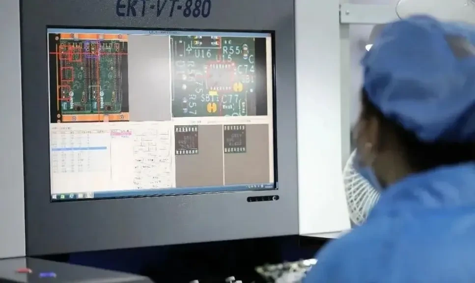
Today we shall discuss the role of AOI inspection in PCBA manufacturing. AOI (Automated Optical Inspection) plays a pivotal role throughout the entire production process of PCBA (Printed Circuit Board Assembly). By combining optical imaging with intelligent algorithms, it achieves efficient and precise defect screening and quality control. The following analysis explores its significance across four dimensions: inspection efficiency, defect identification, process optimisation, and data traceability:
Analysis of the Role of AOI Inspection in PCBA Processing
I. Enhancing Inspection Efficiency and Reducing Labour Costs
Traditional manual inspection relies on visual observation, which is susceptible to factors such as fatigue and variations in experience. This leads to increased rates of missed defects and low efficiency. AOI equipment, however, employs high-resolution cameras to rapidly scan PCB boards. By comparing these scans against pre-set standard images, it enables continuous 24-hour operation with inspection speeds far exceeding manual capabilities. For example:
Client Project Case Study: Following AOI implementation, inspection efficiency increased by 300% while labour costs decreased by 60%. This technology proves particularly advantageous for mass production of high-density, miniaturised PCBs (e.g., mobile phone motherboards, industrial control equipment).
Multi-stage coverage: AOI can be applied throughout the entire production process, including solder paste inspection (SPI), post-placement inspection, and final inspection after reflow soldering, ensuring quality control at every stage.
II. Precise defect identification, reducing rework waste
Through optical imaging and algorithmic analysis, AOI technology detects minute defects invisible to the naked eye, including but not limited to:
Soldering defects: cold solder joints, bridging, cold solder balls, voids, etc.;
Component issues: misplacement, missing components, polarity errors, tombstoning, sideways placement, etc.;
Solder paste printing issues: uneven thickness, positional deviation, missed printing, etc.
Case studies:Kaos Intelligent AOI algorithm model: reduced false alarm rate from 3% to 0.3%, increasing first-pass yield by 70%;
Automotive electronics client: through AOI data analysis, lowered soldering defect rate from 0.5% to 0.08%, significantly reducing rework costs.
III. Optimising Production Workflows to Enhance Overall Efficiency
AOI equipment serves not only for final inspection but can be integrated into production processes for real-time monitoring:
Pre-soldering inspection: Verifies solder paste volume and offset to prevent bridging or cold solder joints;
In-process inspection: Monitors reflow oven temperature zone parameters to ensure soldering quality;
Post-soldering inspection: Identifies complex defects such as missing components or incorrect polarity.
Data-driven optimisation:The AOI system automatically logs defect types, locations, and frequencies, generating SPC (Statistical Process Control) reports. This assists engineers in swiftly pinpointing process weaknesses (e.g., insufficient pick-and-place machine precision, abnormal reflow oven temperature zones), enabling defect prevention rather than reactive rectification.
IV. Supporting Quality Traceability to Meet High Reliability Requirements
During AOI inspection, the inspection data for each PCB board (such as images and defect types) can be archived, fulfilling the quality traceability requirements of high-reliability industries like medical and aerospace. For example:
A new energy electronics PCBA manufacturing process: Through AOI inspection data traceability, production batch issues are rapidly identified and process parameters optimised.
Quality Management System: Inspection data provides evidence for quality improvement, assisting enterprises in establishing robust quality traceability systems.
Ⅴ.Future Trends in AOI Technology
With the integration of AI and big data technologies, AOI is evolving towards intelligent upgrades:
AI Deep Learning: Training models using vast defect datasets enhances recognition accuracy for complex defects (e.g., BGA solder ball voids);
Multi-functional Integration: Combining 3D inspection and X-ray analysis to achieve comprehensive screening of internal component defects;
Predictive Maintenance: Analysing historical data to forecast equipment failure risks, thereby reducing downtime.
Summary
AOI inspection significantly enhances production efficiency and product quality in PCBA manufacturing through efficient, precise defect screening, while simultaneously reducing labour costs and rework waste. Its data-driven optimisation capabilities and quality traceability further meet the demands of high-reliability industries. With ongoing technological advancements, AOI will become an indispensable ‘quality guardian’ in PCBA processing, propelling the industry towards higher quality and greater efficiency.
With 16 years of expertise in PCBA design, manufacturing, and service, KingshengPCBA is ready to help turn your ideas into reality. Feel free to contact us anytime to discuss your requirements and get a professional quotation.

Please send Email to kspcba@c-alley.com or call us through +86 13828766801 Or submit your inquiry by online form. Please fill out below form and attach your manufacturing files( PCB Gerber files and BOM List) if need quotation. We will contact you shortly.
 +86 13828766801
 kspcba@c-alley.com
 https://www.kingshengpcba.com/
 2/F, Building 6, Tangtou 3rd Industrial Zone, Tangtou Community, Shiyan Town, Baoan District, Shenzhen, China, 518108
We would also like to thank our customers for their trust and support. The company's outstanding achievements are mainly due to the loyalty of our customers, which also encourages and spurs our company to forge ahead.


