* On your first PCB Assembly order!
* Up to $300 discount
 C - A L L E Y
 Home | Events | PCB | About Us | News | Contact Us
In the fast-paced world of electronics manufacturing, ensuring the quality of Printed Circuit Board Assemblies (PCBAs) is critical. Defects in PCBAs can lead to product failures, costly recalls, and reputational damage. To mitigate these risks, manufacturers employ a multi-stage quality inspection process, leveraging advanced technologies such as Automated Optical Inspection (AOI), In-Circuit Testing (ICT), Functional Testing (FCT), and X-Ray Inspection.
1. Why Quality Inspection is Essential for PCBAs
PCBA defects can arise from various issues, including:
- Soldering defects (bridges, insufficient solder, cold joints).
- Component misalignment or missing parts.
- Electrical faults (shorts, open circuits).
- Hidden defects (voids in BGA solder joints, internal layer issues).
To catch these defects early, manufacturers implement a structured inspection process that combines automated and manual verification techniques.
2. Key PCBA Quality Inspection Methods
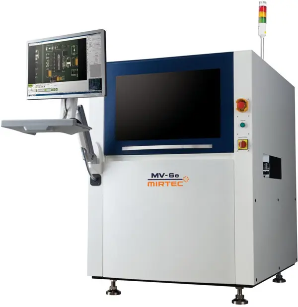
A. Automated Optical Inspection (AOI)
Purpose: Detects surface-level defects such as soldering issues, missing components, and misalignment.
How It Works:
1) High-resolution cameras scan the PCBA and compare it against a reference design.
2) AI algorithms identify deviations (e.g., incorrect polarity, tombstoning).
Advantages: Fast and non-destructive.& Effective for high-volume production.
Limitations: Cannot detect hidden solder joints (e.g., under BGAs).
B. In-Circuit Testing (ICT)
Purpose: Verifies electrical connectivity and component functionality.
How It Works:
1) A bed-of-nails tester probes test points to check for.
2) Shorts/open circuits.
3) Correct resistance, capacitance, and diode functionality.
Advantages: Highly accurate for electrical testing.& Identifies manufacturing defects early.
Limitations: Requires custom test fixtures (increases cost). & Limited to accessible test points.
C. Functional Testing (FCT)
Purpose: Ensures the PCBA operates as intended in real-world conditions.
How It Works:
1) The board is powered up and tested under simulated operating conditions.
2) Firmware and software interactions are verified.
Advantages: Validates overall functionality. & Catches issues missed by AOI/ICT (e.g., firmware bugs).
Limitations: More time-consuming than AOI/ICT.
D. X-Ray Inspection (AXI)
Purpose: Detects hidden defects in solder joints (e.g., BGA, QFN packages).
How It Works:
1) X-rays penetrate the PCB, revealing internal solder connections.
2) Used for: Void detection in solder joints. & Solder ball alignment in BGAs.
Advantages: Non-destructive and highly precise. & Essential for high-density and miniaturized boards.
Limitations: Higher cost than AOI.
3. The Ideal Inspection Workflow
To maximize defect detection, a multi-stage inspection approach is recommended:
- Pre-Assembly Inspection – Verify component authenticity and PCB integrity.
- Post-Reflow AOI – Catch soldering and placement defects.
- ICT/FCT – Confirm electrical and functional performance.
- X-Ray (For Complex Boards) – Inspect hidden solder joints.
- Final Visual & Manual Inspection – Human verification for nuanced defects.
4. Emerging Trends in PCBA Inspection
AI-Powered AOI – Improved defect recognition with machine learning.
3D X-Ray Tomography – Enhanced 3D imaging for complex assemblies.
Automated Flying Probe Testing – Flexible alternative to ICT.
Conclusion
A robust PCBA quality inspection process is vital for minimizing defects and ensuring product reliability. By integrating AOI, ICT, FCT, and X-Ray inspection, manufacturers can achieve near-zero defect rates while optimizing production efficiency. As PCBAs become more complex, leveraging AI-driven inspection and advanced imaging will be key to maintaining high standards in electronics manufacturing.
Need a reliable PCBA partner with stringent quality control? Contact KingshengPCBA today for a consultation!

Please send Email to kspcba@c-alley.com or call us through +86 13828766801 Or submit your inquiry by online form. Please fill out below form and attach your manufacturing files( PCB Gerber files and BOM List) if need quotation. We will contact you shortly.
 +86 13828766801
 kspcba@c-alley.com
 https://www.kingshengpcba.com/
 2/F, Building 6, Tangtou 3rd Industrial Zone, Tangtou Community, Shiyan Town, Baoan District, Shenzhen, China, 518108
We would also like to thank our customers for their trust and support. The company's outstanding achievements are mainly due to the loyalty of our customers, which also encourages and spurs our company to forge ahead.


