* On your first PCB Assembly order!
* Up to $300 discount
 C - A L L E Y
 Home | Events | PCB | About Us | News | Contact Us
In today's wave of electronic products pursuing thinness, shortness, and high performance, High-Density Interconnect (HDI) boards have become the core technology for achieving this goal. As a professional pioneer in the field of electronic manufacturing, we have always stood at the forefront of HDI technology, overcoming one process limit after another.
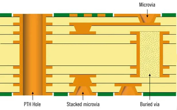
Microvias and Blind/Buried Vias: Core Pillars of HDI Technology
Traditional circuit boards can no longer meet the demand for high-density wiring in modern electronic devices, which is precisely the area where HDI technology shines. Microvia technology, especially microvias with diameters less than 0.15mm, enables us to achieve more connections in a limited space, significantly improving signal transmission efficiency. Blind/buried via technology, on the other hand, achieves three-dimensional wiring by selectively forming connections between different board layers, solving the spatial bottleneck in high-density interconnection.
Our laser drilling technology precisely controls the diameter and depth of microvias, achieving a hole position accuracy of up to ±0.025mm. This ensures stable electrical performance and reliability, even for the most complex multi-layer HDI boards. This precision manufacturing capability provides a solid technical foundation for 5G communications, high-end wearable devices, and medical electronics.
Addressing the Challenges of Miniaturized Components
As miniature components such as 01005 (0.4mm x 0.2mm) and 0201 (0.6mm x 0.3mm) become commonplace, conventional assembly processes face significant challenges. These tiny components demand extremely high placement accuracy, where even minor deviations can lead to connection failures.
We have overcome this challenge through a multifaceted approach:
Precision Stencil Design: Stencils are fabricated using ultra-high precision laser cutting and electro-polishing techniques, maintaining an aperture accuracy within ±0.005mm. Innovatively, we employ stepped stencil technology tailored to different component characteristics. This involves varying the thickness across different regions to precisely control solder paste deposition. Such fine-grained control ensures the uniformity and consistency of micro-component soldering, significantly enhancing assembly yield rates.
Welding Process Breakthrough for Ultra-Fine Pitch BGAs
The advent of BGA components with pitches of 0.3mm or less has propelled electronic assembly technology to new heights. These components have extremely small pin pitches, rendering traditional soldering techniques inadequate.
Our implementation of nitrogen reflow soldering technology has demonstrated exceptional performance in this area.
Performing reflow soldering under a nitrogen atmosphere effectively prevents oxidation of pads and solder balls at high temperatures, significantly improving soldering quality. By precisely controlling the oxygen content in the nitrogen atmosphere (typically below 1000 ppm), we achieve more uniform heat transfer, resulting in more consistent solder joint formation and reducing defects such as open circuits and bridging.
Concurrently, we have developed specialized thermal management strategies for ultra-fine pitch BGAs. By optimizing pad design and heat sink management, we address internal stress issues arising from coefficient of thermal expansion (CTE) mismatch, substantially enhancing the long-term reliability of the products.
Synergistic Effects of Precision Manufacturing
The superior performance of HDI boards relies not only on breakthroughs in individual technologies but also on the precise coordination of each process step.
From substrate selection and pattern transfer to etching control and surface treatment, each step must achieve extreme precision. Our multi-layer registration accuracy is controlled within ±0.025mm, and the line width/spacing can reach 0.05mm/0.05mm. This comprehensive precision manufacturing capability ensures the high reliability and stability of the final product.
In today's rapidly evolving electronics technology landscape, we are consistently dedicated to continuous innovation and breakthroughs in process technology. Your complex designs serve as the ideal platform for us to showcase our technical capabilities. Whether it involves high-density interconnect, micro-component assembly, or ultra-fine pitch BGA applications, we, KingshengPCBA, can provide professional solutions to transform your innovative concepts into reliable, high-performance products.
Pushing the boundaries of manufacturing excellence to shape the future of electronics – let us collaborate to elevate the art of precision manufacturing to unprecedented heights.

Please send Email to kspcba@c-alley.com or call us through +86 13828766801 Or submit your inquiry by online form. Please fill out below form and attach your manufacturing files( PCB Gerber files and BOM List) if need quotation. We will contact you shortly.
 +86 13828766801
 kspcba@c-alley.com
 https://www.kingshengpcba.com/
 2/F, Building 6, Tangtou 3rd Industrial Zone, Tangtou Community, Shiyan Town, Baoan District, Shenzhen, China, 518108
We would also like to thank our customers for their trust and support. The company's outstanding achievements are mainly due to the loyalty of our customers, which also encourages and spurs our company to forge ahead.


