* On your first PCB Assembly order!
* Up to $300 discount
 C - A L L E Y
 Home | Events | PCB | About Us | News | Contact Us
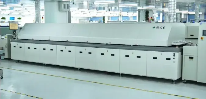
In PCBA manufacturing, reflow soldering is a critical yet challenging process. Studies show that up to 65% of assembly defects originate here, with component tombstoning and solder bridging accounting for nearly 40% of these failures. Optimizing your reflow profile across its four key zones is essential for high-yield production.
The 4 Critical Temperature Zones: A Technical Breakdown
1. Preheat Zone (Ambient to ~150°C)
Purpose: Gradual heating to activate flux and minimize thermal shock.
Key Data: Maintain a ramp rate of 1.0-2.0°C/second. Exceeding 2.5°C/sec increases tombstoning risk by over 300%. Aim for 60-90 seconds in this zone to reduce temperature variance across the board to below 50°C.
2. Soak Zone (~150-200°C)
Purpose: Thermal equalization and flux activation.
Key Data: Hold for 60-120 seconds. Ensure less than 5°C variation across the assembly. Over 70% of tombstoning issues trace back to insufficient or uneven soak times, while 34% of solder bridges are caused by premature solvent boiling from inadequate soaking.
3. Reflow Zone (Peak: 235-250°C for Lead-Free)
Purpose: Solder melting and joint formation.
Key Data: Time Above Liquidus (TAL) should be 45-75 seconds. Peak temperature must stay within component specifications, typically not exceeding 260°C. Note that solder viscosity drops by ~65% upon melting. Maintaining the temperature 15-25°C above liquidus for 30-45 seconds achieves optimal wetting and minimizes bridging.
4. Cooling Zone
Purpose: Controlled solidification for joint integrity.
Key Data: A cooling rate of 2-4°C/second is ideal. Rates faster than 5°C/sec can increase stress fractures by 200%. Controlled cooling promotes a fine-grained joint microstructure, improving mechanical strength by up to 40%.
Practical Guide to Avoiding Defects
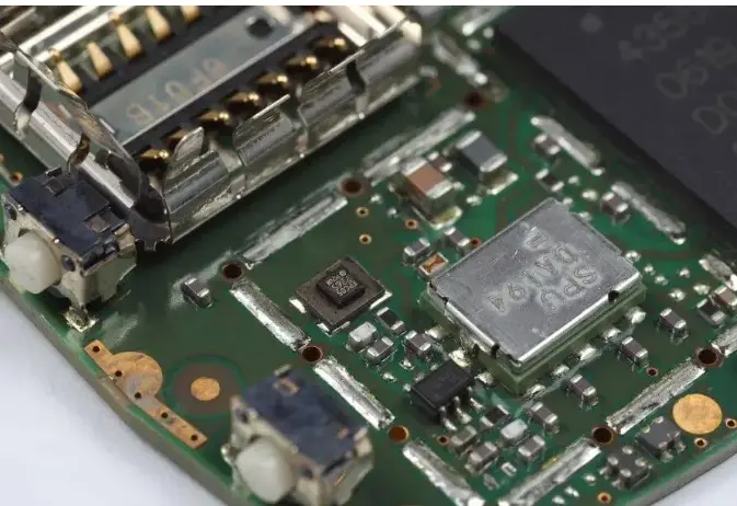
Preventing Tombstoning (Component Lift-off)
Root Cause: Uneven heating or solder paste wetting between a component's two terminals.
Solutions:
1. Optimize Pad Design: Ensure symmetric pad size and thermal relief. The pad size ratio should be between 1:1 and 1:1.2.
2. Refine Stencil Design: For 0201 and smaller components, use an aperture width to pad width ratio of 0.9:1.
3. Control Paste Volume: Keep paste volume variation between paired pads under 8%.
Result: These measures can reduce tombstoning rates from 500 ppm to below 50 ppm.
Eliminating Solder Bridging (Shorts)
Root Cause: Excess solder or incorrect reflow dynamics causing adjacent pins to connect.
Solutions:
1. Upgrade Stencil: Use laser-cut, nano-coated stencils with trapezoidal walls to improve paste release accuracy by 15-20%.
2. Select Proper Paste: For fine-pitch components (<0.5mm pitch), use Type 4 powder (20-38µm).
3. Design with Solder Thieves: Add dummy pads downstream of fine-pitch components to capture excess solder.
Result: This approach can reduce bridging on 0.3mm pitch QFPs from 2.1% to 0.3%.
Key Takeaways for Process Excellence
1. Profile Precisely: Always create a profile based on your specific board's thermal mass, using a minimum of 5 thermocouples.
2. Control the Ramp: Strictly manage the preheat and cooling rates to minimize thermal stress.
3. Design for Manufacturing (DFM): Collaborate with your design team early to implement pad, stencil, and layout optimizations.
4. Monitor and Maintain: Perform regular oven maintenance and thermal profiling to ensure consistent results.
By deeply understanding the science of each reflow zone and implementing these data-driven strategies, manufacturers can dramatically reduce costly defects, improve first-pass yield, and enhance overall product reliability.
KINGSHENGPCBA masters not only the core reflow soldering process but also excels in reducing enterprise costs through digital solutions. From prototype validation at the initial stage to large-scale mass production, also serves as your trusted partner by leveraging advanced nitrogen reflow soldering technology and adaptable service models. We look forward to hearing from you.

Please send Email to kspcba@c-alley.com or call us through +86 13828766801 Or submit your inquiry by online form. Please fill out below form and attach your manufacturing files( PCB Gerber files and BOM List) if need quotation. We will contact you shortly.
 +86 13828766801
 kspcba@c-alley.com
 https://www.kingshengpcba.com/
 2/F, Building 6, Tangtou 3rd Industrial Zone, Tangtou Community, Shiyan Town, Baoan District, Shenzhen, China, 518108
We would also like to thank our customers for their trust and support. The company's outstanding achievements are mainly due to the loyalty of our customers, which also encourages and spurs our company to forge ahead.


