PCBA in IoT Devices: Specific Considerations for Compact Design
 C - A L L E Y
Home | Events | PCB | About Us | News | Contact Us
With the rapid development of IoT technology, we are surrounded by countless small and intelligent devices, ranging from smart home sensors to wearable devices. The design of the printed circuit board assembly (PCBA), the "brain" of these devices, faces challenges not encountered in traditional electronic products. How to achieve high performance, low power consumption, and stable connectivity within a very limited space has become the core issue in PCBA design for IoT devices.
 Extreme Optimization of Size and Layout
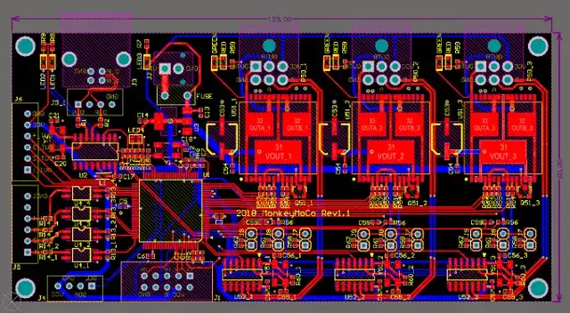
IoT devices typically need to be embedded in confined spaces or portable enclosures, which means that the PCBA must be highly compact. Designers no longer have large spacious layouts, and every square millimeter needs to be carefully planned. Multilayer boards (typically 4-8 layers) have become the standard choice, enabling complex routing through vertical stacking. Component selection also favors miniaturization, with 01005-sized passive components and WLCSP (Wafer Level Chip Scale Package) integrated circuits becoming increasingly common.
More critically, the layout must consider thermal management and signal integrity. In dense layouts, concentrated heat sources can cause localized overheating, affecting device reliability.Simultaneously, the risk of crosstalk between high-frequency signal lines increases, necessitating the use of ground plane shielding and carefully planned trace routing to maintain signal purity.
 Fine-grained Design of Power Consumption Management
Most IoT devices rely on battery power and are expected to have a battery life of months or even years. This necessitates prioritizing power management in PCBA design. Beyond selecting low-power chips, the design of the Power Management Unit (PMU) is particularly critical. Hardware support for multi-voltage domains, smart wake-up circuits, and deep sleep modes must be meticulously implemented at the PCB level.
In compact layouts, power integrity becomes more challenging. The placement of decoupling capacitors and the partitioning design of power planes directly affect the stability of chip power supply.
Inadequate power design can lead to voltage drops, causing abnormal device resets or performance degradation.
The Unique Challenges of Wireless Connectivity
Connectivity is central to the Internet of Things, and the integration of wireless modules is one of the most sensitive aspects of PCBA design. Within a limited space, antenna performance is highly susceptible to the influence of surrounding components and ground planes. PCB antennas or chip antennas require specific clearance areas and should be kept away from metal components and high-speed digital circuits.
Radio frequency (RF) traces necessitate strict 50-ohm impedance control, which demands precise stack-up design and trace width calculation in high-density layouts. Simultaneously, the digital interface between the wireless module and the main processor requires isolation to prevent high-frequency noise from interfering with sensitive RF receiving circuits.
Balance Between Reliability and Manufacturability
Compact designs must not compromise reliability. On miniaturized PCBAs, reduced solder joint sizes exacerbate mechanical stress concentration issues. Designs should avoid placing large Ball Grid Array (BGA) packaged components in stress-sensitive areas, such as near connectors, and consider using underfill to reinforce critical components.
Manufacturability is equally important. BGA chips with ultra-fine pitch may require more advanced soldering processes, such as micro-pitch solder paste printing. The provision of test points also presents challenges. When space is extremely limited, designers must strike a balance between test coverage and layout density, sometimes resorting to indirect testing methods such as boundary scan.
Enhanced Environmental Adaptability Considerations
IoT devices are often deployed in diverse and even harsh environments. Compact PCBA designs imply less housing protection, necessitating enhanced environmental adaptability directly at the circuit board level. This includes using thicker gold plating to prevent oxidation, applying conformal coating to protect against moisture and corrosion, and selecting industrial-grade components with wider operating temperature ranges.
The matching of the coefficient of thermal expansion (CTE) becomes more critical in miniaturized designs. CTE differences between dissimilar materials can lead to solder joint cracking during temperature cycling, affecting long-term reliability.
Conclusion
PCBA design for IoT devices is a precise balancing act performed on a millimeter scale, where every decision involves trade-offs between performance, power consumption, size, and reliability.
Successful compact designs require not only advanced EDA tools and simulation techniques but also a deep understanding of IoT application scenarios by the designer. With the development of new technologies such as flexible circuits and system-in-package (SiP), the design boundaries of IoT PCBAs will continue to expand, but the core principle remains unchanged: to create the most intelligent and reliable connections within the smallest possible space.
In this era of the Internet of Everything, these tiny circuit boards hidden within devices, with their ingenious designs, are quietly supporting the operation of the intelligent world.
With 16 years of expertise in PCBA design, manufacturing, and service, KingshengPCBA is ready to help turn your ideas into reality. Feel free to contact us anytime to discuss your requirements and get a professional quotation.

 +86 13828766801
 kspcba@c-alley.com
 https://www.kingshengpcba.com/
 2/F, Building 6, Tangtou 3rd Industrial Zone, Tangtou Community, Shiyan Town, Baoan District, Shenzhen, China, 518108


