* On your first PCB Assembly order!
* Up to $300 discount
 C - A L L E Y
 Home | Events | PCB | About Us | News | Contact Us
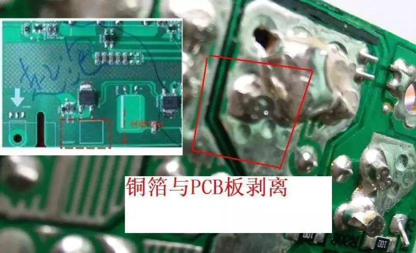
During SMT placement and DIP insertion PCBA soldering processes, PCB delamination (delamination, bubbling, or cracking) is a common manufacturing defect primarily caused by thermal stress, moisture expansion, or material defects. The following outlines systematic preventive and improvement measures.
I. Primary Causes of Delamination
1. Material Issues
1) Moisture absorption in PCB substrate material (e.g., FR-4 moisture absorption exceeding specifications).
2) Insufficient high-temperature resistance in materials with low Tg (glass transition temperature).
3) Poor adhesion between copper foil and substrate (due to inadequate resin systems).
2. Process Issues
1) Excessive soldering temperatures or prolonged exposure times (e.g., peak reflow temperatures exceeding board limits).
2) Abrupt temperature changes (insufficient preheating or accelerated cooling).
3. Design Issues
1) Uneven copper foil distribution (localised thermal stress concentration).
2) Absence of thermal equilibrium design for large copper areas.
4. Storage and Handling
1) PCB stored in humid environments without baking pre-treatment.
2) Cumulative thermal shock from multiple reflow cycles (e.g., DIP insertion after double-sided SMT).
II. Preventive and Remedial Measures
1. Material Optimisation
1) Select high-Tg laminates: Tg ≥ 170°C (Tg ≥ 150°C recommended for lead-free processes) to enhance high-temperature resistance.
2) Low CTE materials: Choose substrates with matched Coefficient of Thermal Expansion (CTE) to minimise thermal stress.
3) Verify supplier quality: Require PCB manufacturers to provide material certifications (e.g., IPC-4101 standard) and test critical parameters including CTE, Tg, and moisture absorption rate.
2. Design Improvements
1) Copper foil uniformity: Avoid localised thick copper areas; employ grid copper or balanced copper designs where necessary.
2) Thermal stress relief design:
Add teardrops or thermal buffer holes to large pads.
Maintain ≥0.3mm spacing between through-holes and copper foil to reduce thermal conduction concentration.
3) Laminate structure optimisation: Employ symmetrical designs for multilayer boards to minimise Z-axis expansion differences.
3. Process Control
1) Strict Temperature and Humidity Management:
PCB Storage Environment: ≤25°C, humidity ≤40% RH (vacuum packaging + desiccator).
Pre-soldering Reflow: 125°C/4-6 hours (adjust according to board thickness) to remove moisture.
2) Optimised Soldering Profiles:
Reflow Soldering: Peak temperature ≤ material limit (e.g., FR-4 typically ≤260°C), heating rate ≤3°C/s.
Wave Soldering: Preheat temperature 80–120°C, soldering time ≤5 seconds.
3) Minimising Thermal Shock Cycles:
Optimise process sequence (e.g., SMT placement before through-hole insertion to avoid multiple reflows).
For double-sided boards, prioritise soldering the side with fewer components.
4. Production Process Monitoring
1) Incoming Material Inspection:
Employ TMA (Thermomechanical Analysis) to test CTE. Conduct cross-section analysis to assess laminate quality.
Perform thermal stress testing on samples (e.g., 288°C/10s solder lift test).
2) Real-time monitoring:
Verify temperature curve consistency using furnace temperature testers (KIC, Datapaq).
Implement SPC statistical control for critical parameters (e.g., peak temperature, heating rate).
3) First article inspection:
Conduct X-ray or cross-section analysis on the first article to check for delamination in inner layers.
5. Additional Critical Measures
1) Lead-Free Process Adaptation: Lead-free soldering requires higher temperatures, necessitating concurrent substrate upgrades (e.g., Isola 370HR, Tuc 862HF).
2) Equipment Maintenance: Regularly calibrate oven temperatures to prevent control deviations caused by thermocouple ageing.
3) Staff Training: Standardise operational procedures (e.g., avoid bare-handed PCB contact to prevent perspiration contamination).
III. Case Study Analysis
Case 1: Edge bubbling on DIP-mounted boards post-wave soldering.
Cause: PCB not oven-dried, moisture absorption rate 0.8% (standard ≤0.2%).
Resolution: After baking, adjusted wave soldering preheat to 110°C, eliminating the issue.
Case 2: Delamination of inner layers on double-sided SMT boards after secondary reflow.
Cause: Board material Tg=130°C, unable to withstand two 260°C reflow cycles.
Resolution: Replaced with Tg=170°C material and optimised layout to single-sided dense component placement.
IV. Conclusion
PCB delamination requires coordinated improvements across multiple dimensions: design, materials, manufacturing processes, and management. The core objectives are to reduce thermal stress, control humidity, and enhance material temperature resistance. Through Design for Manufacturability (DFM) reviews, rigorous incoming material inspections, and optimised process parameters, the risk of delamination can be significantly reduced, thereby improving PCBA yield rates.
With 16 years of expertise in PCBA design, manufacturing, and service, KingshengPCBA is ready to help turn your ideas into reality. Feel free to contact us anytime to discuss your requirements and get a professional quotation.

Please send Email to kspcba@c-alley.com or call us through +86 13828766801 Or submit your inquiry by online form. Please fill out below form and attach your manufacturing files( PCB Gerber files and BOM List) if need quotation. We will contact you shortly.
 +86 13828766801
 kspcba@c-alley.com
 https://www.kingshengpcba.com/
 2/F, Building 6, Tangtou 3rd Industrial Zone, Tangtou Community, Shiyan Town, Baoan District, Shenzhen, China, 518108
We would also like to thank our customers for their trust and support. The company's outstanding achievements are mainly due to the loyalty of our customers, which also encourages and spurs our company to forge ahead.


