* On your first PCB Assembly order!
* Up to $300 discount
 C - A L L E Y
 Home | Events | PCB | About Us | News | Contact Us
The 3W principle for PCB routing is a commonly applied guideline for directing PCB layout and signal trace routing. What do the three Ws represent? They denote three critical aspects: Width (trace width), Waste (unnecessary space), and Weave (trace interweaving).
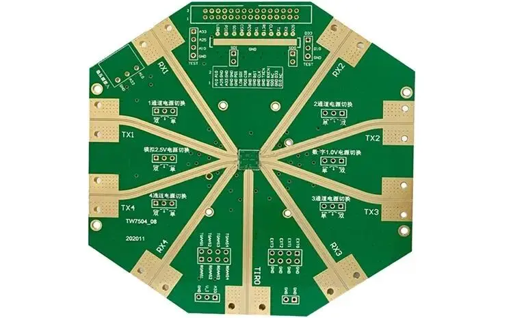
A Detailed Explanation of the 3W Principle
Line width: Select an appropriate line width for signal transmission according to design requirements. Wider line widths reduce resistance and voltage drop, providing superior signal transmission capability. Narrower line widths conserve space and lower manufacturing costs. Determine the suitable line width based on current and specific signal requirements.
Waste: Avoid unnecessary line length wastage. When optimising layout, minimise signal trace lengths and reduce bending or circuitous routing. This mitigates risks of signal propagation delay, crosstalk, and signal distortion.
Interleaving: Interlace signal traces with power/ground traces. By arranging signal and power/ground traces in an alternating pattern within the layout, the potential for electromagnetic interference is reduced. This helps maintain signal integrity and minimises noise impact on signals.
When applying the 3W principle, it is essential to comprehensively consider factors such as signal integrity, electromagnetic compatibility, manufacturability, and space utilisation. Appropriate trace width selection, layout optimisation, and the interweaving of signal and power/ground traces can enhance the quality and performance of PCB designs.
With 16 years of expertise in PCBA design, manufacturing, and service, KingshengPCBA is ready to help turn your ideas into reality. Feel free to contact us anytime to discuss your requirements and get a professional quotation.

Please send Email to kspcba@c-alley.com or call us through +86 13828766801 Or submit your inquiry by online form. Please fill out below form and attach your manufacturing files( PCB Gerber files and BOM List) if need quotation. We will contact you shortly.
 +86 13828766801
 kspcba@c-alley.com
 https://www.kingshengpcba.com/
 2/F, Building 6, Tangtou 3rd Industrial Zone, Tangtou Community, Shiyan Town, Baoan District, Shenzhen, China, 518108
We would also like to thank our customers for their trust and support. The company's outstanding achievements are mainly due to the loyalty of our customers, which also encourages and spurs our company to forge ahead.


