* On your first PCB Assembly order!
* Up to $300 discount
 C - A L L E Y
 Home | Events | PCB | About Us | News | Contact Us
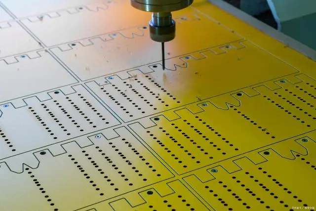
In the design and manufacturing of printed circuit boards (PCBs), the drilling process is a critical step that affects circuit performance, reliability, and manufacturability. Proper design of drilling parameters is not only related to the integrity of signal transmission but also directly determines production efficiency and yield. This article systematically elaborates on the technical key points and common issues in the drilling process from four aspects: aperture compensation, tolerance control, non-metallized hole treatment, and positioning hole design, aiming to provide practical reference for engineering designers.
Aperture Compensation
The primary consideration in the drilling process is the aperture size and its compensation. Since the minimum drill bit diameter for mechanical drilling is typically 0.2mm, and the copper thickness of the hole wall and the thickness of the protective layer need to be considered during the production process, the actual drilling diameter needs to be appropriately increased based on the design.
For instance, tin-sprayed boards typically require an increase of 0.15mm, while gold-plated boards need an increase of 0.1mm. This compensation measure introduces a critical issue: after the hole diameter is increased, does the safety distance between the hole and the surrounding traces or copper areas still meet the process requirements? Of particular concern is whether the annular ring width is sufficient. For example, if the designed via hole diameter is 0.2mm and the pad diameter is 0.35mm, the theoretical single-sided annular ring width is 0.075mm, which can still meet the processing requirements. However, if it is a tin-sprayed board and the hole diameter is increased, the annular ring may disappear completely. If the pad cannot be enlarged due to routing density limitations, the board may become unproducible.
Tolerance Control
Hole diameter tolerance and the isolation distance between holes and inner layer patterns are also crucial considerations.
Currently, the processing tolerance of drilling rigs in China is generally controlled within ±0.05mm. After adding the plating thickness tolerance, the total tolerance for metallized holes is approximately ±0.075mm, while for non-metallized holes, it is about ±0.05mm. Furthermore, it is necessary to consider the drilling positioning tolerance (±0.075mm) and the expansion and contraction deformation of the inner layer patterns during lamination (±0.1mm). Therefore, to ensure production feasibility and reliability, the spacing from the hole edge to the inner layer lines or copper foil in the design should be at least 0.15mm for 4-layer boards and 0.2mm or more for 6-layer boards and above.
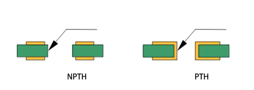
NPTH Treatment
The production of non-plated through holes (NPTH) typically involves methods such as dry film sealing, resin plugging, and secondary drilling. It should be noted that dry film sealing is generally suitable for hole diameters not exceeding 6.0mm, while resin plugging is not recommended for diameters smaller than 11.5mm.
Regardless of the process used, a copper-free area of 0.2mm around NPTH should be maintained to prevent electrical shorts or signal interference.
Positioning Holes Design
The design of positioning holes is often overlooked. In testing, routing, or milling processes, holes with a diameter greater than 1.5mm are typically required as fixed positioning holes. It is recommended to arrange them in a triangular pattern at the three corners of the PCB to improve processing stability and alignment accuracy.
Conclusion
The drilling process is a critical and comprehensive step in PCB manufacturing that demands high precision. Designers must comprehensively consider multiple factors, including aperture compensation, tolerance control, and NPTH treatment, positioning holes design, and make reasonable plans based on actual production conditions.
Only by fully anticipating and mitigating process risks during the design phase can the manufacturability and reliability of the circuit board be effectively improved, ensuring that the product is successfully put into production and meets performance requirements. Through scientific design methods and rigorous process control, the drilling process will become an important support for ensuring PCB quality and stability.
Thank you for reading. We hope this article provided valuable insights for you.
With 16 years of expertise in PCBA design, manufacturing, and service, KingshengPCBA is ready to help turn your ideas into reality. Feel free to contact us anytime to discuss your requirements and get a professional quotation.

Please send Email to kspcba@c-alley.com or call us through +86 13828766801 Or submit your inquiry by online form. Please fill out below form and attach your manufacturing files( PCB Gerber files and BOM List) if need quotation. We will contact you shortly.
 +86 13828766801
 kspcba@c-alley.com
 https://www.kingshengpcba.com/
 2/F, Building 6, Tangtou 3rd Industrial Zone, Tangtou Community, Shiyan Town, Baoan District, Shenzhen, China, 518108
We would also like to thank our customers for their trust and support. The company's outstanding achievements are mainly due to the loyalty of our customers, which also encourages and spurs our company to forge ahead.


