* On your first PCB Assembly order!
* Up to $300 discount
 C - A L L E Y
 Home | Events | PCB | About Us | News | Contact Us
With the rapid advancement of the PCB industry, an increasing number of engineering and technical personnel are entering the field of circuit board design and manufacturing. However, due to the complexity of PCB production processes and the multitude of manufacturing steps involved, many designers, lacking practical manufacturing experience, often prioritize electrical performance and functional realization in their designs, while neglecting manufacturability considerations. This can lead to processing difficulties, delays in production cycles, and even potential quality issues in downstream manufacturing. To enhance design-manufacturing collaboration efficiency, this paper will analyze key design considerations for board thickness and copper thickness:
Board Thickness Key Design Considerations
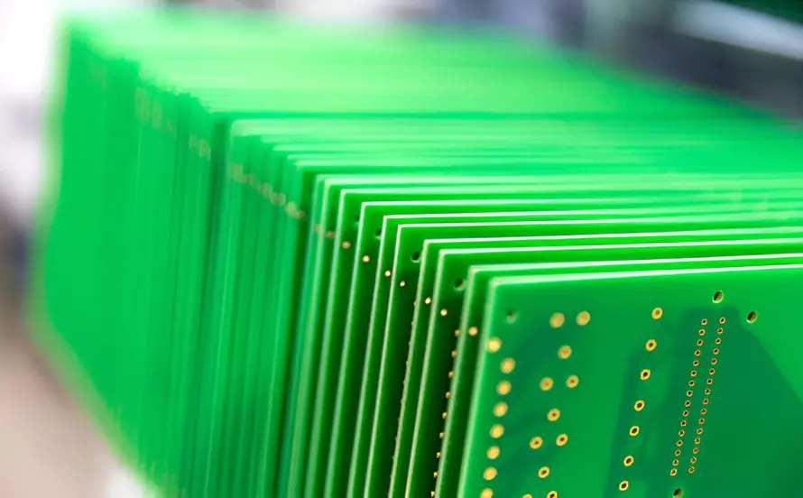
In the PCB cutting-material stage, the selection of board thickness needs to consider both standard and customized requirements. Conventional board thicknesses are categorized into standard series: ≥0.8mm series (such as 1.0, 1.6, and 2.0mm) and <0.8mm series (such as 0.2, 0.4, and 0.6mm). The latter is often used for inner core boards in multilayer PCBs. It should be noted in the design that the finished board thickness will increase due to the superposition of outer layer processes. For example, copper plating, solder mask, surface treatment (such as HASL and ENIG), and character printing will all contribute to thickness accumulation. Typically, the actual board thickness increases by approximately 0.05–0.15mm compared to the design value. Therefore, if the finished product has strict thickness limitations, it is necessary to consider using non-standard laminates (e.g., selecting a 1.9mm base material when the design target is 2.0mm), but this will extend the procurement and delivery cycle.
Board Thickness Tolerance Control
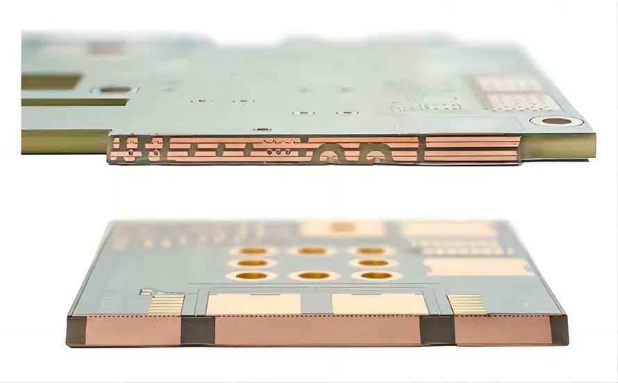
Board thickness tolerance control is critical for ensuring assembly compatibility and is influenced by three factors: the tolerance of the raw board material, lamination tolerance, and outer layer processing tolerance. Standard board thickness tolerances are generally as follows: (0.8–1.0) mm ±0.10 mm, (1.2–1.6) mm ±0.13 mm, 2.0 mm ±0.18 mm, and 3.0 mm ±0.23 mm. Lamination tolerance is typically controlled within a range of ±(0.05–0.10) mm. Particularly when designing PCBs with edge connectors (e.g., gold fingers), the thickness and tolerance must be precisely specified according to the mechanical mating requirements of the connector to ensure reliable insertion.
Copper Thickness Key Design Considerations
Regarding copper thickness design, comprehensive planning is necessary, considering both the electroplating process and IPC standards. Hole copper and surface copper increase in thickness simultaneously during electroplating. According to IPC-A-600G, the minimum hole copper thickness for Class 1 and 2 boards is 20 μm, while for Class 3 boards, it is 25 μm.
In actual production, to balance electrical performance and manufacturing feasibility, a "thin substrate + plating" strategy is often used to achieve the target copper thickness. For example, if the required finished copper thickness is 1OZ (approximately 35μm), a 1/2OZ (approximately 17.5μm) substrate can be selected for blanking. After plating, the total copper thickness can reach approximately 33–36μm, which not only meets the electrical requirements but also facilitates the fabrication of fine lines. This method is particularly important in high-layer count and high-density designs.
Conclusion
This paper systematically elucidates the key design principles of the PCB blanking stage regarding board thickness and copper thickness from the perspective of Design for Manufacturing (DFM). It is recommended that designers introduce manufacturing constraints in the initial layout stage and establish a regular communication mechanism with the process front-end. This approach achieves an optimal balance among electrical performance, structural adaptation, and production feasibility, thereby optimizing Product Quality, cost, and Delivery cycle as a whole, and promoting the continuous development of the PCB industry towards high integration and high reliability.
With 16 years of expertise in PCBA design, manufacturing, and service, KingshengPCBA is ready to help turn your ideas into reality. Feel free to contact us anytime to discuss your requirements and get a professional quotation.

Please send Email to kspcba@c-alley.com or call us through +86 13828766801 Or submit your inquiry by online form. Please fill out below form and attach your manufacturing files( PCB Gerber files and BOM List) if need quotation. We will contact you shortly.
 +86 13828766801
 kspcba@c-alley.com
 https://www.kingshengpcba.com/
 2/F, Building 6, Tangtou 3rd Industrial Zone, Tangtou Community, Shiyan Town, Baoan District, Shenzhen, China, 518108
We would also like to thank our customers for their trust and support. The company's outstanding achievements are mainly due to the loyalty of our customers, which also encourages and spurs our company to forge ahead.


