* On your first PCB Assembly order!
* Up to $300 discount
 C - A L L E Y
 Home | Events | PCB | About Us | News | Contact Us
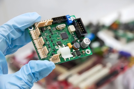
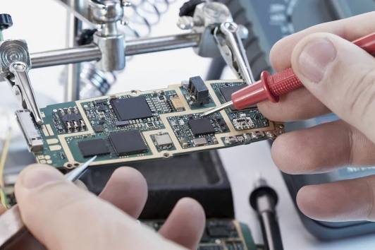
In the precision-driven world of PCBA (Printed Circuit Board Assembly) manufacturing, solder paste printing stands as the most critical step in the SMT process. As electronic designs evolve toward greater complexity—combining ultra-fine-pitch components with large-power devices—traditional stencils often prove inadequate. This is where 3D step stencil technology emerges as a game-changing solution, enabling unparalleled process control for advanced assemblies.
Understanding the Technology and Its Drivers
A 3D step stencil is a specialized laser-cut stencil fabricated with varying thicknesses across its surface. Unlike a conventional stencil of uniform thickness, it features precisely engineered raised (step-up) or recessed (step-down) areas. This sophisticated approach is increasingly necessary in modern PCBA due to the prevalence of mixed-technology boards. It is common to find a single design incorporating 0.3mm pitch micro-BGAs, 0402 passives, and large QFNs or connectors. A single-thickness stencil forces a compromise on paste volume, inevitably leading to defects—bridging on fine-pitch components or insufficient solder on high-mass terminations.
Key Applications in Advanced PCBA Production
The deployment of 3D step stencils is targeted and strategic, addressing specific SMT challenges:
Managing Diverse Solder Volume Requirements: This is the primary application. The stencil is locally thickened (stepped-up) in areas feeding large components, such as connectors or power ICs, to deposit additional paste for robust mechanical and electrical bonds. Simultaneously, it remains at a standard thickness for fine-pitch components to prevent bridging. This eliminates the need for a secondary printing process, thereby maximizing PCBA line throughput.
Correcting for PCB Topography: Advanced designs often feature non-planar surfaces due to embedded components or varied copper densities. A step stencil can be contoured to compensate for these height variations, ensuring consistent gasketing and uniform paste release across the entire board. This capability is vital for achieving high yields in cutting-edge PCBA applications.
Mitigating Passive Component Defects: For tiny chip components like 0201 or 01005, uneven paste volume is a leading cause of tombstoning. A strategically placed step-down region can reduce the paste volume and the resultant vertical separation force, effectively suppressing this common defect.
Implementation and Process Considerations
Successfully integrating 3D step stencils requires meticulous attention to detail:
Fabrication Method: Steps can be created through chemical etching (for step-down) or precise laser welding (for step-up). The method impacts cost, lead time, and the sharpness of the transition.
Transition Zone Design: The ramp between different thickness levels must be smooth and gradual. A well-designed transition, typically with a controlled slope, is crucial to prevent paste scooping and ensure a clean squeegee pass.
Enhanced Process Control: Utilizing a step stencil necessitates a robust and stable printing process. Adjustable squeegee pressure and speed are essential to accommodate the varying surface height. Furthermore, implementing 3D Solder Paste Inspection (SPI) is mandatory to verify that the correct volume has been deposited in each distinct zone of the PCBA.
Conclusion
The adoption of 3D step stencil technology represents a significant advancement in SMT process capability for the PCBA industry. It provides an elegant and highly effective solution for managing the complex solder paste requirements of modern mixed-technology boards. By enabling precise, variable paste deposition in a single print cycle, it directly drives higher first-pass yields, reduces soldering defects, and facilitates the assembly of more innovative and compact products. For any PCBA manufacturer aiming to excel in the assembly of complex boards, mastering 3D step stencil technology is not just an option; it is a strategic imperative for achieving manufacturing excellence.
Thank you for reading. We hope this article provided valuable insights for you. With 16 years of expertise in PCBA design, manufacturing, and service, KingshengPCBA is ready to help turn your ideas into reality. Feel free to contact us anytime to discuss your requirements and get a professional quotation.

Please send Email to kspcba@c-alley.com or call us through +86 13828766801 Or submit your inquiry by online form. Please fill out below form and attach your manufacturing files( PCB Gerber files and BOM List) if need quotation. We will contact you shortly.
 +86 13828766801
 kspcba@c-alley.com
 https://www.kingshengpcba.com/
 2/F, Building 6, Tangtou 3rd Industrial Zone, Tangtou Community, Shiyan Town, Baoan District, Shenzhen, China, 518108
We would also like to thank our customers for their trust and support. The company's outstanding achievements are mainly due to the loyalty of our customers, which also encourages and spurs our company to forge ahead.


