* On your first PCB Assembly order!
* Up to $300 discount
 C - A L L E Y
 Home | Events | PCB | About Us | News | Contact Us
You've spent weeks on design, sourcing, and assembly. The board powers on... sometimes. It passes tests... intermittently. You find yourself chasing a phantom—a glitch that appears and vanishes with temperature, vibration, or no apparent reason at all. After countless frustrating hours, you finally spot it: a single, seemingly innocuous solder joint that looks dull, grainy, and poorly formed.
This is the cold solder joint. It's not a complete failure, but a flawed connection that lurks within your PCBA, waiting to wreak havoc. In this post, we'll dissect this most insidious of defects, exploring its root causes, its staggering hidden costs, and arming you with a comprehensive strategy to eliminate it from your products for good.
What Exactly is a Cold Solder Joint?
Beyond a simple "bad connection," a cold solder joint (or "intermittent solder connection") occurs when the solder fails to melt completely and form a proper metallurgical bond with the component lead and PCB pad. Instead of a strong, shiny, continuous connection, it results in a weak, high-resistance, and often cracked interface.
Think of it like this: A proper solder joint is a solid weld. A cold solder joint is a piece of tape barely holding two parts together. It might maintain contact under ideal conditions, but any stress—thermal expansion, mechanical shock, current surge—can break that fragile connection, causing an instantaneous, and often temporary, failure.
The Staggering Hidden Cost of Cold Joints
Why are cold joints so feared? Because their cost extends far beyond the price of a little extra solder.
Exorbitant Debugging & Rework: Finding one cold joint among thousands of good ones is a needle-in-a-haystack endeavor. It consumes invaluable engineering time that could be spent on innovation.
Catastrophic Field Failures: A product that fails after deployment triggers a cascade of costs: returns, warranty repairs, service calls, and shipping.
Irreparable Brand Damage: Nothing erodes customer trust faster than an unreliable product. Cold joints create the "it just stops working" perception that can destroy a brand's reputation.
Contrast with Other Defects: A short circuit is often obvious and caught during testing. A missing component is easy to spot. A cold joint is a stealthy saboteur that can slip through quality control and activate in the customer's hands.
The Root Causes: A Failure Across the PCBA Process
Cold solder joints are rarely the fault of a single step; they are often the result of a chain of minor process failures.
1. Design (DFM) Origins:
Poor Thermal Balance: A large ground plane connected to a small component lead acts as a heat sink, drawing heat away during reflow and preventing the solder from fully melting.
Incorrect Pad Geometry: Pads that are too small or have improper spacing can hinder good solder wetting and fillet formation.
2. Material Issues:
Component/PCB Oxidation: Exposed copper pads or component leads can oxidize, creating a barrier that the solder cannot penetrate.
Poor Solder Paste Quality: Using old, oxidized, or low-activity solder paste prevents proper fluxing and wetting, directly leading to cold joints.
3. The Manufacturing Process (The Main Culprit):
- Solder Paste Printing: Insufficient paste volume due to a clogged stencil or incorrect pressure will result in a weak, incomplete joint.
- Component Placement: Misalignment or insufficient placement force can lead to an unbalanced joint.
- Reflow Soldering (The Critical Stage): This is where most cold joints are born.
- Insufficient Preheat: Failing to properly activate the flux leads to oxidation during the peak reflow phase.
- Too-Rapid Thermal Ramp: Can cause solder splatter and incomplete flux activation.
- Insufficient Peak Temperature/Time Below Liquidus (TAL): If the solder doesn't spend enough time above its melting point, it cannot fully wet the surfaces and will re-solidify into a cold, granular structure.
Hunting the Ghost: How to Detect Cold Solder Joints
This is a challenge because cold joints often pass electrical tests in a static environment.
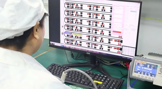
Automatic Optical Inspection (AOI): Can flag joints with a dull, grainy, or non-shiny appearance, but is not foolproof.
X-Ray Inspection: Essential for finding voids or cracks in BGA balls and other hidden joints, which are a form of cold joint.
In-Circuit Test (ICT) & Flying Probe: Typically ineffective, as they may make a good electrical connection during the test.
The Most Effective Methods:
1. Manual Visual Inspection (MVI): A trained inspector with a microscope looks for the characteristic dull, porous, and cracked appearance.
2. Functional Testing with Stress: The most reliable way to find intermittents. This involves running the board through a functional test while subjecting it to controlled vibration (e.g., on a shake table) or thermal cycling. The stress breaks the weak connection, revealing the fault.
3. Building Your Defense: A Proactive Prevention Strategy
The only way to win the battle against cold joints is to prevent them from ever forming.
4. Design for Excellence (DFM/DFA):
Use thermal relief patterns for pads connected to large copper pours to balance heat dissipation.
Follow IPC standards for pad and stencil design.
5. Stringent Material Control:
Implement proper storage and shelf-life management for PCBs and solder paste to prevent oxidation.
Perform regular solder paste quality checks.
6. Process Mastery & Control:
Reflow Profiling is Key. This is your #1 weapon. Create and validate a robust reflow profile for every unique board. Use a profiling thermocouple attached to the most challenging thermal mass points (like a large ground pad) to ensure the entire board reaches the necessary temperature and time above liquidus (TAL). Re-verify this profile regularly.
7. Optimize Solder Paste Printing: Monitor print quality with SPI (Solder Paste Inspection) to ensure consistent volume and alignment.
Conclusion: A Battle Won by Process, Not Luck
Cold solder joints are not a matter of bad luck; they are a failure of process control. By understanding their multifaceted causes—from your CAD software to your reflow oven—you can transform this elusive threat into a manageable variable.
Thank you for reading. We hope this article provided valuable insights for you. With 16 years of expertise in PCBA design, manufacturing, and service, KingshengPCBA is ready to help turn your ideas into reality. Feel free to contact us anytime to discuss your PCBA requirements and get a professional quotation.

Please send Email to kspcba@c-alley.com or call us through +86 13828766801 Or submit your inquiry by online form. Please fill out below form and attach your manufacturing files( PCB Gerber files and BOM List) if need quotation. We will contact you shortly.
 +86 13828766801
 kspcba@c-alley.com
 https://www.kingshengpcba.com/
 2/F, Building 6, Tangtou 3rd Industrial Zone, Tangtou Community, Shiyan Town, Baoan District, Shenzhen, China, 518108
We would also like to thank our customers for their trust and support. The company's outstanding achievements are mainly due to the loyalty of our customers, which also encourages and spurs our company to forge ahead.


