* On your first PCB Assembly order!
* Up to $300 discount
 C - A L L E Y
 Home | Events | PCB | About Us | News | Contact Us
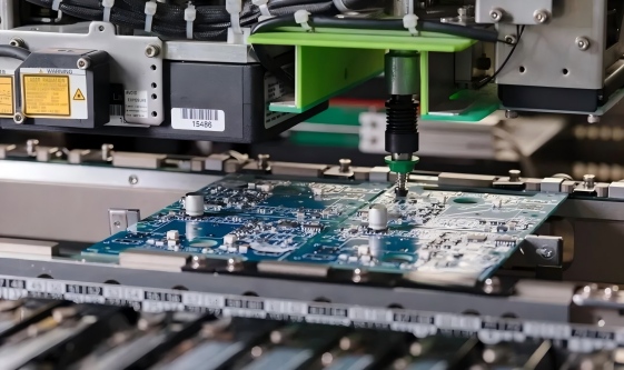
In the complex landscape of PCBA (Printed Circuit Board Assembly) manufacturing, wave soldering remains a crucial process for through-hole components, yet it consistently presents a significant challenge: solder shorts. These unintended bridges between adjacent pins or leads represent one of the most common and costly defects in PCBA production, leading to electrical failures, increased rework costs, and compromised product reliability. While process parameter optimization can provide some improvement, the most effective approach begins with strategic Design for Manufacturability (DFM) principles.
Understanding the Root Causes in the PCBA Context
The persistence of solder shorts in PCBA lines often stems from fundamental design limitations that conflict with wave soldering physics. Component shadowing represents a primary challenge, where larger upstream components disrupt solder flow to downstream pins, creating turbulent zones that promote bridging. Similarly, inadequate pin-to-pin spacing fails to provide sufficient clearance for clean solder separation, particularly problematic with fine-pitch connectors and multi-lead components. These issues are further compounded by suboptimal pad geometries and insufficient solder mask definition between terminals.
Strategic DFM Improvement Solutions
1. Optimized Component Layout and Orientation
The single most impactful DFM strategy involves orienting all components so their longer axis runs parallel to the board's direction of travel through the solder wave. This simple adjustment minimizes shadowing effects and ensures uniform solder exposure. Additionally, maintaining generous spacing between sensitive components – particularly fine-pitch connectors – creates the physical separation necessary for clean solder separation. For high-density PCBA designs, this may require strategic component placement across both board sides.
2. Implementation of Solder Thieving Technology
For multi-lead components where bridging frequently occurs, incorporating robber pads (solder thieves) at the trailing edge of component footprints provides a targeted solution. These non-functional copper pads serve as sacrificial destinations, capturing excess solder that would otherwise form bridges between the last functional pins. This proven technique has demonstrated remarkable effectiveness in eliminating end-pin shorts throughout the PCBA industry.
3. Precision Pad and Solder Mask Design
Refining basic land pattern designs significantly impacts solder short prevention. Adopting oval or teardrop-shaped pads instead of circular configurations provides improved solder exit geometry. More critically, ensuring robust solder mask dams between adjacent pins creates essential physical barriers against solder bridging. The mask registration and thickness must be strictly controlled to achieve consistent results across the PCBA panel.
4. Comprehensive Thermal Management
Balancing the thermal mass across the PCBA panel prevents localized temperature variations that contribute to solder defects. Implementing balanced copper distribution and considering the thermal demands of large ground planes helps maintain consistent solderability across all through-hole connections.
Conclusion: A Proactive Approach to PCBA Excellence
Addressing wave solder shorts requires a fundamental shift from reactive process adjustments to proactive DFM integration. By implementing these design-based strategies – optimal component orientation, solder thieving technology, precision pad design, and thermal balance – PCBA manufacturers can transform their quality metrics. This DFM-focused approach not only reduces short circuits but also decreases rework requirements, improves first-pass yield, and enhances overall product reliability.
In today's competitive electronics manufacturing landscape, mastering these DFM principles represents not just a technical advantage but a crucial business imperative for delivering high-quality PCBA products.
Thank you for reading. We hope this article provided valuable insights for you.
With 16 years of expertise in PCBA design, manufacturing, and service, KingshengPCBA is ready to help turn your ideas into reality. Feel free to contact us anytime to discuss your requirements and get a professional quotation.

Please send Email to kspcba@c-alley.com or call us through +86 13828766801 Or submit your inquiry by online form. Please fill out below form and attach your manufacturing files( PCB Gerber files and BOM List) if need quotation. We will contact you shortly.
 +86 13828766801
 kspcba@c-alley.com
 https://www.kingshengpcba.com/
 2/F, Building 6, Tangtou 3rd Industrial Zone, Tangtou Community, Shiyan Town, Baoan District, Shenzhen, China, 518108
We would also like to thank our customers for their trust and support. The company's outstanding achievements are mainly due to the loyalty of our customers, which also encourages and spurs our company to forge ahead.


