* On your first PCB Assembly order!
* Up to $300 discount
 C - A L L E Y
 Home | Events | PCB | About Us | News | Contact Us
Surface finish selection for PCBs is a critical yet often underestimated decision that impacts solderability, signal integrity, reliability, and manufacturing costs. As modern electronics push toward higher density, faster speeds, and stricter environmental compliance, understanding surface finishes becomes non-negotiable. Here's how to navigate this complex landscape.
Why Surface Finish Matters
The surface finish:
1. Prevents copper oxidation
2. Enables solder joint formation
3. Impacts signal loss at high frequencies
4. Determines rework capability
5. Influences shelf life
A poorly chosen finish can lead to field failures, increased return rates, and costly redesigns.
Comparative Analysis of Key Finishes
1. HASL (Hot Air Solder Leveling)
Pros: Low cost ($0.05-$0.15/dm²), robust solder joints
Cons: Poor planarity (±25µm variation), thermal stress risk
Best for: Cost-driven consumer electronics with components >0.65mm pitch
2. ENIG (Electroless Nickel Immersion Gold)
Pros: Excellent planarity (±1µm), oxidation resistance, Al/Au wire-bondable
Cons: 30-50% cost premium, "Black Pad" failure risk (Ni-P hyper-corrosion)
Ideal Applications: Medical devices, servers, RF modules
3. OSP (Organic Solderability Preservative)
Pros: RoHS-compliant, cheapest lead-free option ($0.02-$0.10/dm²)
Cons: 6-month shelf life, single-reflow limit, invisible to AOI
Dominates: High-volume mobile/consumer PCBs
4. Immersion Silver (ImAg)
Pros: Superior high-frequency performance (skin effect optimized)
Cons: Susceptible to sulfur tarnishing, handling gloves are mandatory
Niche: 5G/mmWave PCBs, antenna substrates
5. Immersion Tin (ImSn)
Pros: Flat surface, excellent for press-fit connectors
Cons: Tin whisker growth risk (JESD201A compliance needed)
Use Cases: Automotive control units, industrial connectors
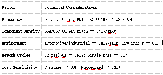
5 Critical Selection Criteria
Emerging Trends & Hybrid Solutions
ENEPIG (Electroless Ni/Electroless Pd/Immersion Au):
Solves "Black Pad" issue while enabling Al/Au wire bonding
Costs 10-15% less than ENIG with comparable reliability
Hybrid Finishes:
Example 1: ENIG on BGA pads + OSP on routing areas (cost optimization)
Example 2: Hard gold fingers (5-50µ") + ImSn on solderable areas
Ultra-Thin Finishes:
Sub-0.1µm gold layers for HDI boards in wearables
Failure Prevention Checklist
HASL: Verify coplanarity for QFN/BGA components
ENIG: Require Ni thickness 3-6µm, P content 7-11%
OSP: Enforce <6hrs exposure before reflow
ImAg: Use nitrogen-sealed packaging
ImSn: Conduct tin whisker testing per JESD22-A121
The Cost-Reliability Tradeoff
While OSP costs ~$0.05/dm² vs. ENIG’s ~$0.30/dm², consider hidden expenses:
-ENIG reduces rework rates by 40-60% vs. OSP
-HASL-related planarity issues cause 15% assembly defects
-Field failures in automotive applications cost 100x the PCB value
Future Outlook
With 5G/6G and AI hardware demanding:
-Low-loss dielectrics → ImAg dominance
-2.5D/3D packaging → ENEPIG adoption
-Sustainability → Halogen-free OSP evolution
The Bottom Line
There's no universal "best" finish – only the optimal choice for your design constraints. Prioritize signal needs, environmental specs, and lifecycle requirements over upfront cost. As Moore's Law pushes interconnects to atomic scales, your surface finish decision may well determine the product's success or failure.
"A $0.20 surface finish can scrap a $20,000 assembly. Choose like it matters."

Please send Email to kspcba@c-alley.com or call us through +86 13828766801 Or submit your inquiry by online form. Please fill out below form and attach your manufacturing files( PCB Gerber files and BOM List) if need quotation. We will contact you shortly.
 +86 13828766801
 kspcba@c-alley.com
 https://www.kingshengpcba.com/
 2/F, Building 6, Tangtou 3rd Industrial Zone, Tangtou Community, Shiyan Town, Baoan District, Shenzhen, China, 518108
We would also like to thank our customers for their trust and support. The company's outstanding achievements are mainly due to the loyalty of our customers, which also encourages and spurs our company to forge ahead.


