* On your first PCB Assembly order!
* Up to $300 discount
 C - A L L E Y
 Home | Events | PCB | About Us | News | Contact Us
In the precision-driven world of Printed Circuit Board Assembly (PCBA), solder joints form the critical backbone of electronic functionality. These microscopic connections dictate electrical performance, mechanical resilience, and long-term reliability. While manual soldering retains niche applications, quantifiable data reveals a significant and widening quality gap between human-performed and machine-driven processes in volume production environments. This divergence stems from inherent limitations in human consistency versus engineered precision.
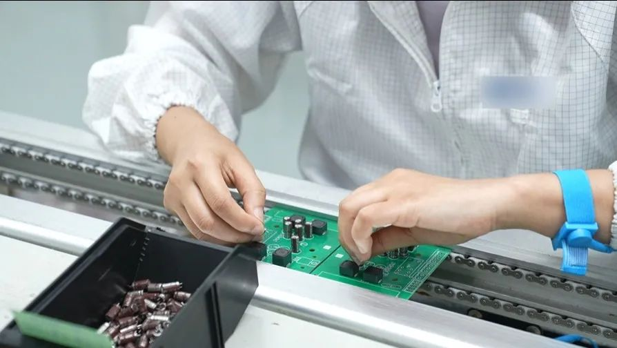
The Human Factor: Variability as the Core Limitation
Manual soldering relies entirely on operator skill, introducing unavoidable variability:
Defect rates typically exceed 5,000–10,000 defects per million opportunities (DPPM) in volume production, compared to <500 DPPM for automated lines.
Consistency challenges: Even skilled technicians struggle to maintain optimal iron angle, dwell time (1-3 seconds), and solder volume across hundreds of joints daily. Fatigue and subjective judgment lead to cold joints, bridging (especially on fine-pitch components), and tombstoning.
Inspection limitations: Visual inspection misses up to 25% of hidden defects like subsurface voids or micro-cracks under components, whereas automated X-ray screening achieves near-100% coverage.
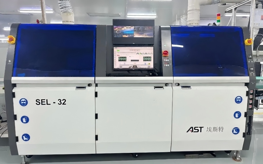
Machine Soldering: Precision Engineered into the Process
Modern automated systems leverage technology to eliminate variability:
Reflow/Selective Soldering: Multi-zone ovens apply scientifically optimized thermal profiles tailored to specific alloys, minimizing thermal shock while ensuring robust intermetallic compound (IMC) formation. Nitrogen environments reduce oxidation, increasing joint strength by 30%.
Closed-loop control: Real-time monitoring of temperature, conveyor speed, and solder wave parameters maintains tolerances impossible for human operators. Integrated Solder Paste Inspection (SPI) ensures paste volume accuracy within ±5%.
Zero-defect ecosystems: Combining SPI pre-reflow, Automated Optical Inspection (AOI) post-reflow, and Automated X-ray Inspection (AXI) for hidden joints drives defect escape rates below 0.1%.
Quantifying the Gap: Beyond Defect Rates
Process Capability (Cp/Cpk): Machine processes consistently achieve Cp/Cpk >1.33 (indicating high statistical control), while manual methods operate at far lower and unstable levels.
Field Reliability: Optimized IMC formation and minimized voids in machine-soldered joints reduce field failure rates by orders of magnitude—critical for automotive, medical, and aerospace applications.
Cost of Quality: One manufacturer reported a 93% reduction in defects (from 52,000 DPPM to 3,500 DPPM) and monthly labor savings of ¥32,000 after automation 3. Similarly, AI-driven inspection systems now cut "overkill" false rejection rates by 50%, boosting throughput.
Where Manual Soldering Endures (and Why)
Despite its disadvantages, manual soldering remains vital for:
-Rework/Repair: Correcting machine defects or field failures (requiring IPC-7711/7721-certified skill).
-Prototyping: Quick iterations without stencil or program setup.
-Extreme odd-form components: Geometries defying current automation, like certain flex circuits or ceramic substrates.
Conclusion: The Future is Automated and Augmented
The data leaves little room for debate: machine soldering delivers superior consistency, traceability, and reliability at scale. Innovations like laser ball placement (enabling 99.7% yield on 0.3mm-pitch BGAs ) and AI-driven process control are widening this gap further. While the artisan's touch remains irreplaceable for rework and niche applications, the trajectory for volume PCBA manufacturing is clear—precision, repeatability, and data-driven optimization are the domain of the machine. Embracing this shift isn't just about efficiency; it's about achieving the near-zero-defect standard demanded by next-generation electronics.
In the calculus of quality, human hands cannot compete with engineered precision.

Please send Email to kspcba@c-alley.com or call us through +86 13828766801 Or submit your inquiry by online form. Please fill out below form and attach your manufacturing files( PCB Gerber files and BOM List) if need quotation. We will contact you shortly.
 +86 13828766801
 kspcba@c-alley.com
 https://www.kingshengpcba.com/
 2/F, Building 6, Tangtou 3rd Industrial Zone, Tangtou Community, Shiyan Town, Baoan District, Shenzhen, China, 518108
We would also like to thank our customers for their trust and support. The company's outstanding achievements are mainly due to the loyalty of our customers, which also encourages and spurs our company to forge ahead.


